H27UBG8T2BTA データシートの表示(PDF) - Hynix Semiconductor
部品番号
コンポーネント説明
一致するリスト
H27UBG8T2BTA Datasheet PDF : 57 Pages
| |||
Preliminary
H27UBG8T2BTR-BC Series
32Gb(4096M x 8bit) Legacy MLC NAND Flash
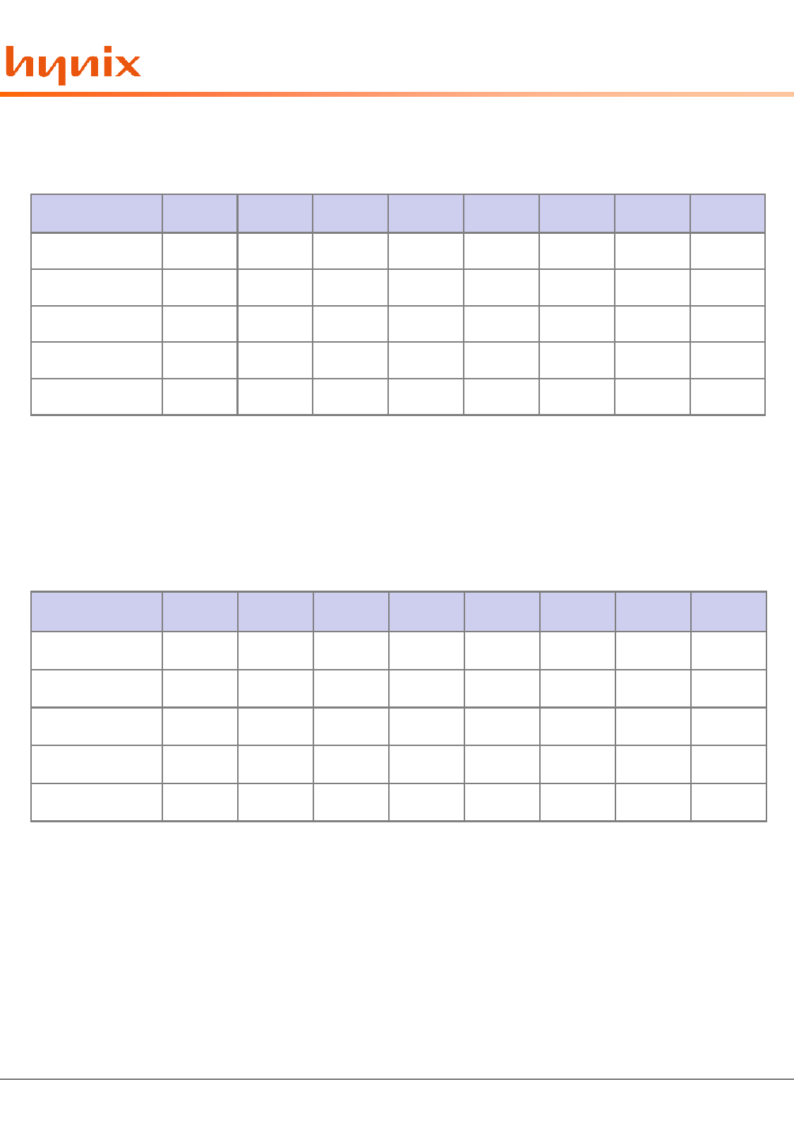
1.7. Addressing
1.7.1. Addressing(MLC mode)
Bus cycle
I/O0
I/O1
I/O2
I/O3
I/O4
I/O5
I/O6
I/O7
1st Cycle
A0
A1
A2
A3
A4
A5
A6
A7
2nd Cycle
A8
A9
A10
A11
A12
A13
L(1)
L(1)
3rd Cycle
A14
A15
A16
A17
A18
A19
A20
A21
4th Cycle
A22
A23
A24
A25
A26
A27
A28
A29
5th Cycle
A30
A31
A32
L(1)
L(1)
L(1)
L(1)
L(1)
Notes:
1. L must be set to Low.
2. The device ignores any additional address input cycle than required.
3. The Address consists of column address (A0~A13), page address (A14 ~ A21), plane address (A22),
and block address (A23 ~ the last address).
1.7.2. Addressing(SLC mode)
Bus cycle
1st Cycle
2nd Cycle
3rd Cycle
4th Cycle
5th Cycle
I/O0
A0
A8
A14
A22
A30
I/O1
A1
A9
A15
A23
A31
I/O2
A2
A10
A16
A24
L(1)
I/O3
A3
A11
A17
A25
L(1)
I/O4
A4
A12
A18
A26
L(1)
I/O5
A5
A13
A19
A27
L(1)
I/O6
A6
L(1)
A20
A28
L(1)
I/O7
A7
L(1)
A21
A29
L(1)
Notes:
1. L must be set to Low.
2. The device ignores any additional address input cycle than required.
3. The Address consists of column address (A0~A13), page address (A14 ~ A20), plane address (A21),
and block address (A22 ~ the last address).
Rev 0.7 / Jan. 2011
11
Share Link: 