VT82C596 データシートの表示(PDF) - Unspecified
部品番号
コンポーネント説明
一致するリスト
VT82C596 Datasheet PDF : 96 Pages
| |||
:H &RQQHFW 7HFKQRORJLHV ,QF
VT82C596B
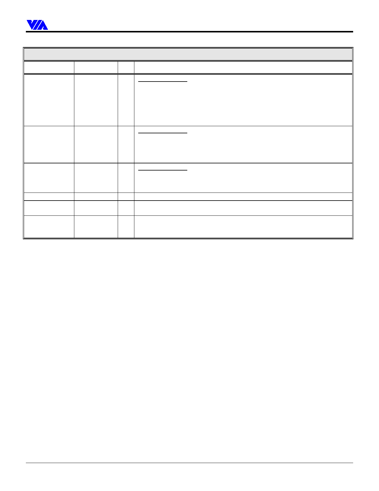
Signal Name
XDIR# / GPO22
XOE# / GPO23
KBCS# / GPO26
ROMCS#
MCCS#
PCS[1-0]#
Pin #
M3
M4
K1
K2
N4
N5, L4
XD Interface
I/O Signal Description
O MultiFunction Pin
X-Bus Data Direction. (Rx75[6]=0) Asserted low for all I/O read cycles and for
memory read cycles to the programmed BIOS or APIC address space. XDIR# is
tied directly to the direction control of a 74F245 transceiver that buffers the X-Bus
data and ISA-Bus data. SD0-7 connect to the “A” side of the transceiver and
XD0-7 connect to the “B” side. XDIR# high indicates that SD0-7 drives XD0-7.
General Purpose Output 22. (Rx75[6]=1) General purpose output.
O MultiFunction Pin
X-Bus Output Enable. (Rx75[6]=0) Asserted low for all decoded X-Bus cycles.
XOE# is tied directly to the output enable of a 74F245 transceiver that buffers the
X-Bus data and ISA-Bus data (see XDIR# above).
General Purpose Output 23. (Rx75[6]=1) General purpose output.
O MultiFunction Pin
External Keyboard Controller Chip Select. (Rx76[2] = 0) Asserted during read
or write accesses to I/O ports 60h and 64h.
General Purpose Output 26. (Rx76[2]=1) General purpose output.
O ROM Chip Select. Chip Select to the BIOS ROM.
O Microcontroller Chip Select. Asserted during read or write accesses to I/O ports
62h or 66h.
O Programmable Chip Selects. Asserted during I/O cycles to programmable read or
write ISA address ranges. Devices selected by these pins are assumed to be on the X-
Bus (XDIR# and XOE# are enabled).
Revision 0.3 June 17, 1999
-13-
Pinouts
Share Link: 