VT82C596 データシートの表示(PDF) - Unspecified
部品番号
コンポーネント説明
一致するリスト
VT82C596 Datasheet PDF : 96 Pages
| |||
:H &RQQHFW 7HFKQRORJLHV ,QF
VT82C596B
Signal Name
REQ[A-C]# / GPI[2-4]
GNT[A-C]# / GPO[9-11]
SERIRQ / GPI7
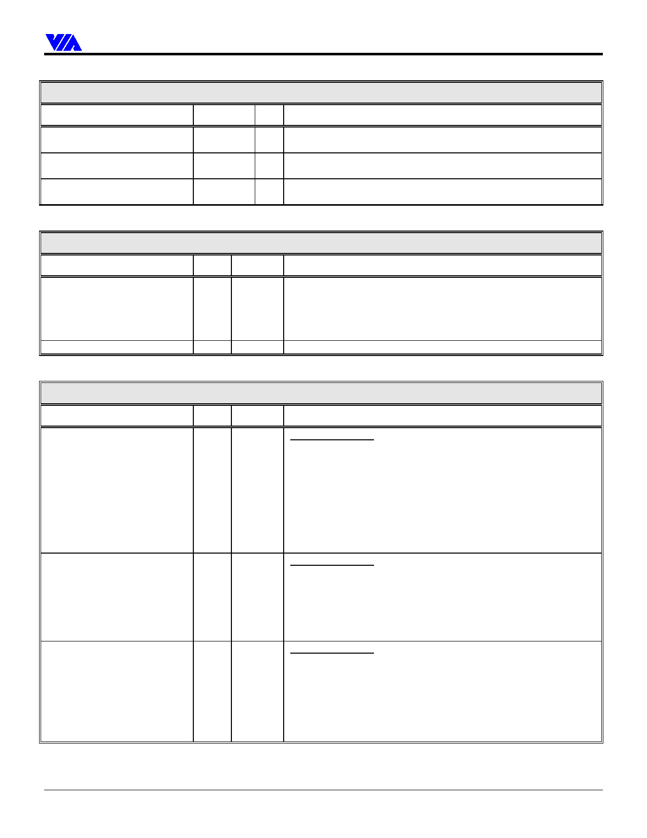
PC/PCI and Serial IRQ Control
Pin # I/O Signal Description
M1, N2, P3 I PC/PCI DMA Requests. Used by PCI agent to request DMA services
per the PC/PCI protocol. For GPI functions refer to Rx7D[2-0].
N1, P2, P4 O PC/PCI DMA Grants. Used to acknowledge DMA services per the
PC/PCI protocol. For GPO functions refer to Rx7D[2-0].
J19
I Serial Interrupt Request. Used with Distributed DMA. For GPI see
Rx68[3].
Signal Name
A20GATE / MSCK
A20M#
Pin #
P1
M20
A20 Control
I/O Signal Description
I
Gate A20: Gate A20 output from optional external keyboard controller
if used. Logically combined with Port 92 bit-1 (Fast_A20) and output
on the A20M# signal. If the internal keyboard / PS2 mouse controller is
used, this pin becomes the mouse clock input (the A20GATE signal
comes directly from the internal keyboard controller).
OD A20 Mask. Connect to A20 mask input of the CPU.
APIC Interface
Signal Name
APICREQ# / WSC# / GPI5
APICCS# / APICD0 / GPO13
APICACK# / APICD1 / GPO12
Pin #
K18
H18
J17
I/O Signal Description
I/I/I
O/O/O
O/O/O
MultiFunction Pin
Internal APIC Write Snoop Complete. (Rx74[7]=1 & Rx74[1]=1)
Asserted by the north bridge to indicate that all snoop activity on the
CPU bus initiated by the last PCI-to-DRAM write is complete and
that it is safe to perform an APIC interrupt.
External APIC Request. (Rx74[7]=1 & Rx74[1]=0) Asserted by
external APIC synchronous to PCICLK prior to sending an interrupt
over the APIC serial bus. This signals the VT82C596B to flush its
internal buffers.
General Purpose Input 5. (Rx74[7] = 0)
MultiFunction Pin
Internal APIC Data 0. (Rx74[7]=1 & Rx74[1]=1)
External APIC Chip Select. (Rx74[7]=1 & Rx74[1]=0) The
VT82C596B drives this signal active to select an external APIC (if
used). This occurs if the external APIC is enabled and a PCI cycle is
detected within the programmed APIC address range.
General Purpose Output 13. (Rx74[7] = 0)
MultiFunction Pin
Internal APIC Data 1. (Rx74[7]=1 & Rx74[1]=1)
External APIC Acknowledge. (Rx74[7]=1 & Rx74[1]=0) Asserted by
the VT82C596B to indicate that it internal buffers have been flushed
(in response to APICREQ#). This indicates to the external APIC that
the VT82C596B’s internal buffers have been flushed and that it is OK
for the APIC to send its interrupt.
General Purpose Output 12. (Rx74[7] = 0)
Revision 0.3 June 17, 1999
-15-
Pinouts
Share Link: 