VT82C596 データシートの表示(PDF) - Unspecified
部品番号
コンポーネント説明
一致するリスト
VT82C596 Datasheet PDF : 96 Pages
| |||
:H &RQQHFW 7HFKQRORJLHV ,QF
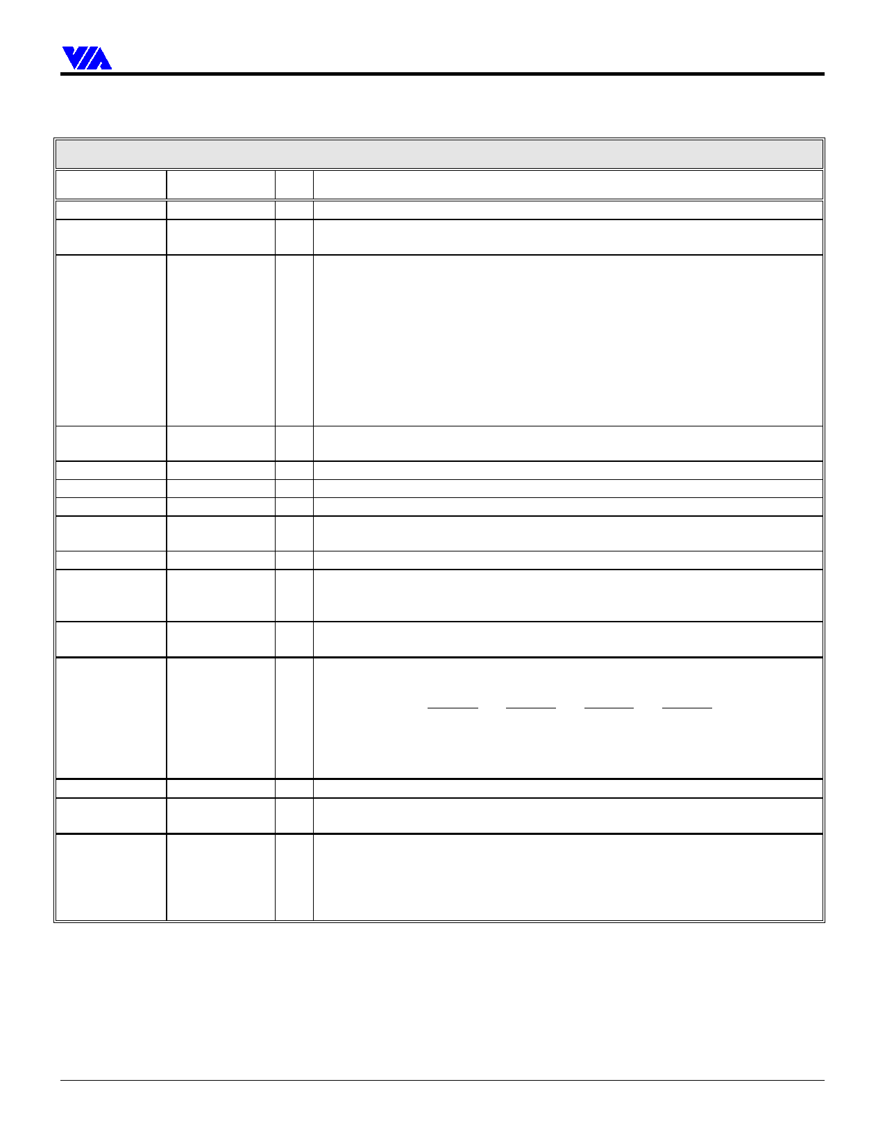
Table 1. Pin Descriptions
VT82C596B
Signal Name
PCLK
FRAME#
AD[31:0]
C/BE[3:0]#
IRDY#
TRDY#
STOP#
DEVSEL#
PAR
SERR#
IDSEL
PIRQA-D#
PREQ#
PGNT#
PCKRUN#
PCI Bus Interface
Pin #
I/O Signal Description
D11
I PCI Clock. PCLK provides timing for all transactions on the PCI Bus.
A5
IO Frame. Assertion indicates the address phase of a PCI transfer. Negation indicates
that one more data transfer is desired by the cycle initiator.
B1, C1, E1,
D1, A2, B2,
IO Address/Data Bus. The standard PCI address and data lines. The address is driven
with FRAME# assertion and data is driven or received in following cycles.
C2, E2, B3, C3,
E3, D3, A4,
B4, C4, E4, E6,
D6, A7, B7,
C7, D7, A8,
B8, E8, D8,
A9, B9, C9,
D9, A10, B10
D2, D4, C6, C8 IO Command/Byte Enable. The command is driven with FRAME# assertion. Byte
enables corresponding to supplied or requested data are driven on following clocks.
B5
IO Initiator Ready. Asserted when the initiator is ready for data transfer.
C5
IO Target Ready. Asserted when the target is ready for data transfer.
D5
IO Stop. Asserted by the target to request the master to stop the current transaction.
E5
IO Device Select. The VT82C596B asserts this signal to claim PCI transactions through
positive or subtractive decoding.
B6
IO Parity. A single parity bit is provided over AD[31:0] and C/BE[3:0]#.
A6
I System Error. SERR# can be pulsed active by any PCI device that detects a system
error condition. Upon sampling SERR# active, the VT82C596B can be programmed
to generate an NMI to the CPU.
A3
I Initialization Device Select. IDSEL is used as a chip select during PCI
configuration read and write cycles.
R3, R4, P5, G1 I PCI Interrupt Request. These pins are typically connected to the PCI bus INTA#-
INTD# pins as follows:
PIRQA# PIRQB# PIRQC# PIRQD#
PCI Slot 1 INTA# INTB# INTC# INTD#
PCI Slot 2 INTB# INTC# INTD# INTA#
PCI Slot 3 INTC# INTD# INTA# INTB#
PCI Slot 4 INTD# INTA# INTB# INTC#
B12
O PCI Request. This signal goes to the North Bridge to request the PCI bus.
A12
I PCI Grant. This signal is driven by the North Bridge to grant PCI access to the
VT82C596B.
C10
IO PCI Bus Clock Run. This signal indicates whether the PCI clock is or will be
stopped (high) or running (low). The VT82C596B drives this signal low when the
PCI clock is running (default on reset) and releases it when it stops the PCI clock.
External devices may assert this signal low to request that the PCI clock be restarted
or prevent it from stopping. Refer to the PCI Mobile Design Guide for more details.
Revision 0.3 June 17, 1999
-7-
Pinouts
Share Link: 