ZR36067 データシートの表示(PDF) - Unspecified
部品番号
コンポーネント説明
一致するリスト
ZR36067 Datasheet PDF : 48 Pages
| |||
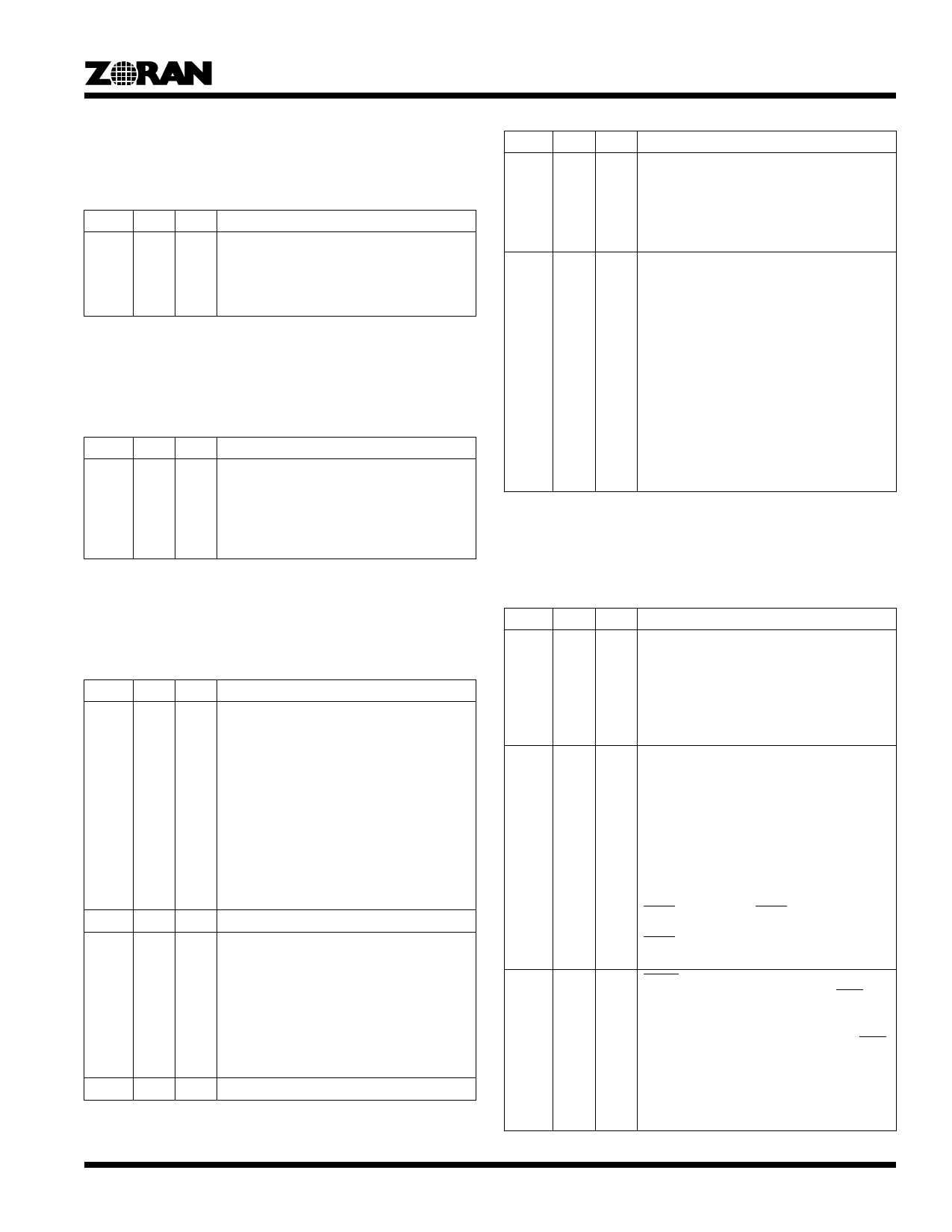
AV PCI CONTROLLER
13.4 Video Display “Top” Register
This register contains the doubleword base address of the top
field.
Address Offset: 0x00C
Bit Type Mod
Description
31:2 RW vid VidTopBase - Video Top Field Base
1:0
R
Address. This is the destination starting
address for the top field.
Default value is 0xFFFFFFFC.
Bits 1..0 are hardwired to 00b.
13.5 Video Display “Bottom” Register
This register contains the doubleword base address of the
bottom field.
Address Offset: 0x010
Bit Type Mod
Description
31:2 RW vid VidBotBase - Video Bottom Field Base
1:0
R
Address.
This is the destination starting address for the
bottom field.
Default value is 0xFFFFFFFC.
Bits 1..0 are hardwired to 00b.
13.6 Video Stride, Status and Frame Grab Register
This register contains parameters for display addressing (bytes
2-3), status of VFIFO (byte 1) and frame grab control (byte 0).
Address Offset: 0x014
Bit Type Mod
Description
31:18 RW
17:16 R
15:9 R
8
RC
7:2
R
vid DispStride - Display Stride.
This register defines the address increment in
bytes to be added to the address of the last
pixel of a display line, to generate the address
of the next consecutive display line.
If the address difference between two con-
secutive display lines is zero (i.e, they are
physically consecutive) than DispStride
should be set (by the driver software) to zero
(if DispMode=1) or to the display line size in
bytes (if DispMode=0).
Default value is 0xFFFC.
Bits 1..0 are hardwired to 00b.
Reserved. Returns zero.
all VidOvf - Video FIFO Overflow flag.
This bit is asserted by the Video FIFO server
when an overflow of the Video FIFO occurs.
This bit is cleared when the host tries to write
‘1’ to it.
In case of concurrent accesses to this bit, it
remains ‘1’.
‘1’ - a VFIFO overflow occurred.
‘0’ - no overflow (default value).
Reserved. Returns zero.
Address Offset: 0x014
Bit Type Mod
Description
1 RW all SnapShot - Frame Grab Mode.
If this bit is asserted the ZR36067 goes into
frame grab mode. When deasserted continu-
ous display of video is resumed.
‘1’ - frame grab mode.
‘0’ - continuous display mode (default value).
0
RS snap FrameGrab - Frame Grabbing Command/
Status.
When this bit is asserted by the host and
SnapShot is asserted, the ZR36067 will
transfer the next two fields (indicated by the
VSYNC signal) to memory. At the end of the
second field this bit will be cleared internally,
indicating that the frame grabbing has been
completed and video transfer has been
stopped.
In case of concurrent accesses to this bit, the
result is ‘0’.
‘1’ - start frame grabbing.
‘0’ - frame grabbing completed (default
value).
13.7 Video Display Configuration Register
This register contains the configuration parameters for the video
display.
Address Offset: 0x018
Bit Type Mod Description
31 RW
30:24 RW
24 RW
all VidEn - Video Display Enable.
If this bit is cleared by the host, video write
DMA transfers are disabled. When enabled,
the video DMA controller operates normally.
‘1’ - normal video transfer mode.
‘0’ - video write transfers disabled (default
value).
vid MinPix - Minimum Number of doublewords.
This parameter defines a threshold value.
When the number of doublewords inside the
Video FIFO has reached this value a video-
write burst is requested.
Default value is 0x0F.
Range 0x01 - 0x3C.
The l.s. bit of this field (bit 24) is also used to
configure the platform PCI bridge type, so the
actual resolution of MinPix is limited by the
Triton bit. When the Triton bit is ‘1’, only odd
values of MinPix are supported. When the
Triton bit is ‘0’, only even values are
supported.
vid Triton - PCI Bridge Controller type.
This parameter configures the PCI REQ
behavior to match the platform PCI bridge
characteristics.
‘0’ - Intel ‘Triton’ Bridge Controller. The REQ
assertion and de-assertion conditions are
modified accordingly.
‘1’ - Other PCI Bridge Controllers.
Default value is ‘1’.
This bit is also used as the l.s. bit of MinPix.
27
Share Link: 