IDT82V2048 データシートの表示(PDF) - Integrated Device Technology
部品番号
コンポーネント説明
一致するリスト
IDT82V2048 Datasheet PDF : 61 Pages
| |||
IDT82V2048 OCTAL T1/E1 SHORT HAUL LINE INTERFACE UNIT
INDUSTRIAL TEMPERATURE RANGES
PIN DESCRIPTION (CONTINUED)
Name
A4
MC3/A3
MC2/A2
MC1/A1
MC0/A0
Type
I
Pin No.
QFP144 BGA160
Description
12
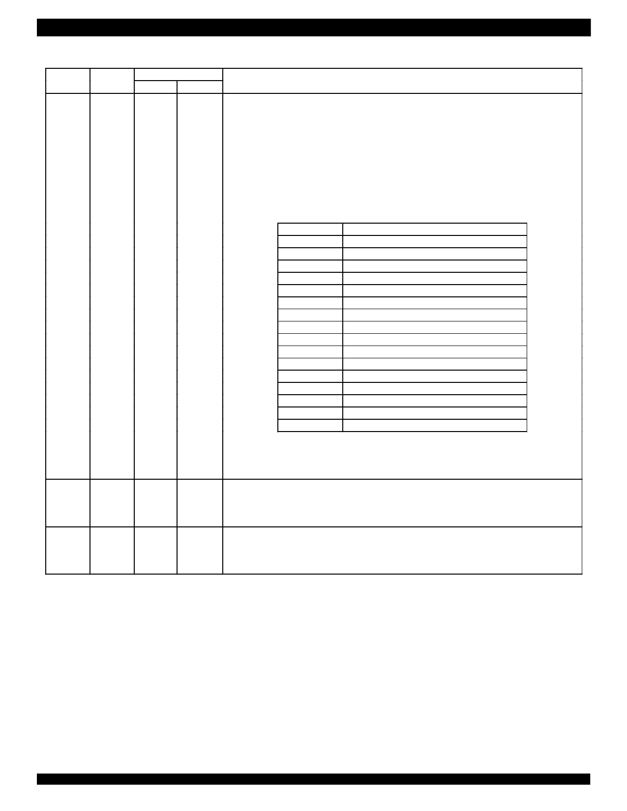
F4 MCn: Performance Monitor Configuration 4~0
13
F3 In hardware control mode, A4 must be connected to GND. MC[3:0] are used to select one
14
F2 transmitter or receiver of the channel 1 to 7 for non-intrusive monitoring. Channel 0 is used as
15
F1 the monitoring channel. If a transmitter is monitored, signals on the corresponding pins TTIPn
16
G3 and TRINGn are internally transmitted to RTIP0 and RRING0. If a receiver is monitored, signals
on the corresponding pins RTIPn and RRINGn are internally transmitted to RTIP0 and RRING0.
The clock and data recovery circuit in receiver 0 can then output the monitored clock to pin
RCLK0 as well as the monitored data to RDP0 and RDN0 pins. The signals monitored by
channel 0 can be routed to TTIP0/TRING0 by activating the remote loopback in this channel.
Performance Monitor Configuration determined by MC[3:0] is shown below. Note that if
MC[2:0] = 000, the device is in normal operation of all the channels.
MC[3:0]
Monitoring Configuration
0000
Normal operation without monitoring.
0001
Monitoring receiver 1.
0010
Monitoring receiver 2.
0011
Monitoring receiver 3.
0100
Monitoring receiver 4.
0101
Monitoring receiver 5.
0110
Monitoring receiver 6.
0111
Monitoring receiver 7.
1000
Normal operation without monitoring.
1001
Monitoring transmitter 1.
1010
Monitoring transmitter 2.
1011
Monitoring transmitter 3.
1100
Monitoring transmitter 4.
1101
Monitoring transmitter 5.
1110
Monitoring transmitter 6.
1111
Monitoring transmitter 7.
OE
I
CLKE
I
An: Address Bus 4~0
When pin MODE1 is low, the parallel host interface operates with separate address and data
bus. In this mode, the signal on this pin is the address bus of the host interface.
114
E14 OE: Output Driver Enable
Pulling this pin to low can make all driver output into high impedance state immediately for
redundancy application without external mechanical relays. In this condition, all the other
internal circuits remain active.
115
E13 CLKE: Clock Edge Select
The signal on this pin determines the active edge of RCLKn and SCLK in clock recovery mode,
or determines the active level of RDPn and RDNn in the data recovery mode. (Refer to
Functional Description and Table-2).
10
Share Link: 