DS2148 データシートの表示(PDF) - Maxim Integrated
部品番号
コンポーネント説明
一致するリスト
DS2148 Datasheet PDF : 73 Pages
| |||
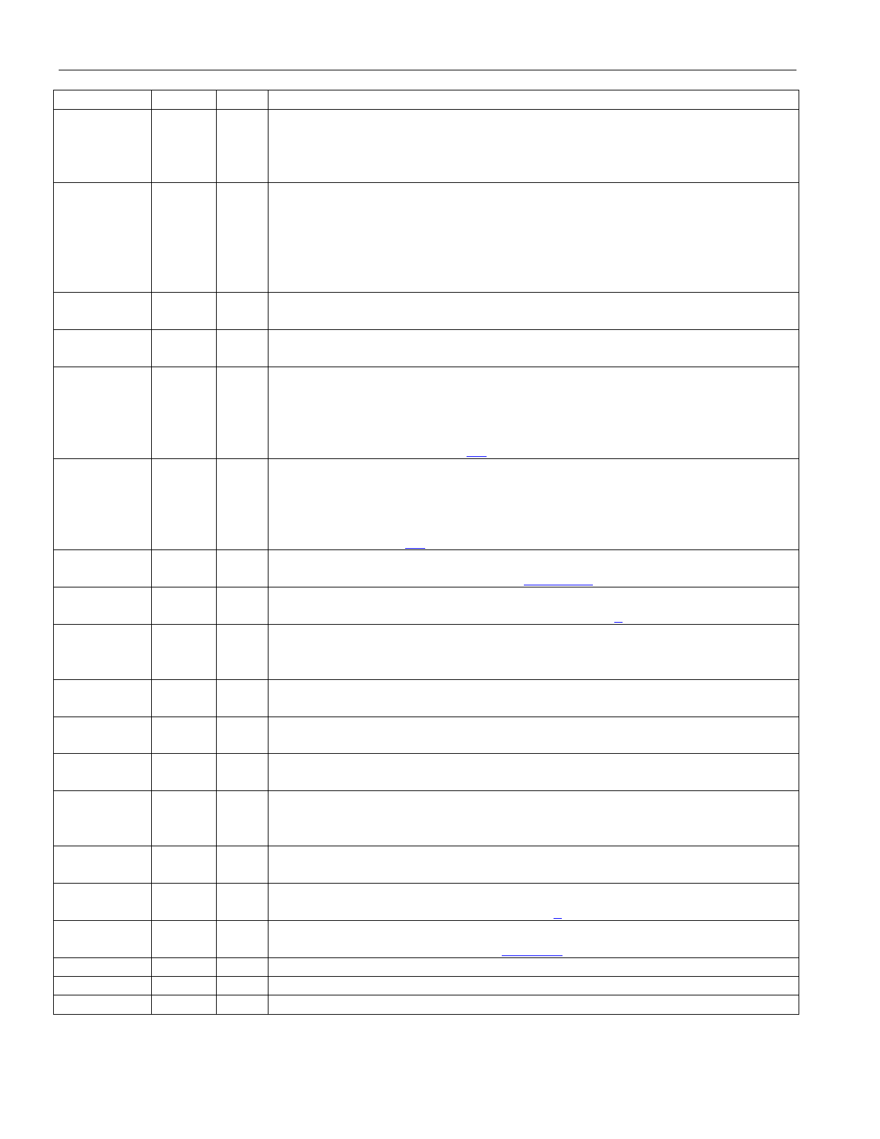
DS2148/DS21Q48
NAME
PIN I/O
FUNCTION
NRZ Enable [H/W Mode]
NRZE
3
I
0 = Bipolar data at RPOS/RNEG and TPOS/TNEG
1 = NRZ data at RPOS and TPOS or TNEG; RNEG outputs a positive going
pulse when device receives a BPV, CV, or EXZ.
PRBS Bit Error Output. The receiver will constantly search for a QRSS (T1)
or a 215-1 (E1) PRBS depending on whether T1 or E1 mode is selected. Remains
PBEO
24
O
high if out of synchronization with the PRBS pattern. Goes low when
synchronized to the PRBS pattern. Any errors in the received pattern after
synchronization will cause a positive going pulse (with same period as E1 or T1
clock) synchronous with RCLK.
RCLK
40
O
Receive Clock. Buffered recovered clock from the line. Synchronous to MCLK
in absence of signal at RTIP and RRING.
RCL
25
O
Receive Carrier Loss. An output which will toggle high during a receive carrier
loss.
Receive Negative Data. Updated on the rising edge (CES = 0) or the falling
edge (CES = 1) of RCLK with the bipolar data out of the line interface. Set
RNEG
39
O NRZE to a one for NRZ applications. In NRZ mode, data will be output on
RPOS while a received error will cause a positive-going pulse synchronous with
RCLK at RNEG. See Section 6.4 for details.
Receive Positive Data. Updated on the rising edge (CES = 0) or the falling edge
(CES = 1) of RCLK with bipolar data out of the line interface. Set NRZE pin to a
RPOS
38
O one for NRZ applications. In NRZ mode, data will be output on RPOS while a
received error will cause a positive-going pulse synchronous with RCLK at
RNEG. See Section 6.4 for details.
RT0/RT1 44/23
I
Receive LIU Termination Select Bits 0 & 1 [H/W Mode]. These inputs
determine the receive termination. See Table 2-12.
RTIP/
RRING
27/28
I
Receive Tip and Ring. Analog inputs for clock recovery circuitry. These pins
connect via a 1:1 transformer to the line. See Section 5 for details.
Receive & Transmit Synchronization Clock Enable.
SCLKE
4
I 0 = disable 2.048MHz synchronization transmit and receive mode
1 = enable 2.048MHz synchronization transmit and receive mode
TCLK
43
I
Transmit Clock. A 2.048MHz or 1.544MHz primary clock. Used to clock data
through the transmit side formatter.
TEST
26
I
Tri-State Control. Set high to tri-state all outputs and I/O pins (including the
parallel control port). Set low for normal operation. Useful in board level testing.
TNEG
42
I
Transmit Negative Data. Sampled on the falling edge (CES = 0) or the rising
edge (CES = 1) of TCLK for data to be transmitted out onto the line.
Transmit Power-Down
TPD
13
I 0 = normal transmitter operation
1 = powers down the transmitter and tri-states the TTIP and TRING pins
TPOS
41
I
Transmit Positive Data. Sampled on the falling edge (CES = 0) or the rising
edge (CES = 1) of TCLK for data to be transmitted out onto the line.
TTIP/
TRING
34/37
O
Transmit Tip and Ring. Analog line driver outputs. These pins connect via a
step-up transformer to the line. See Section 5 for details.
TX0/TX1 14/15
I
Transmit Data Source Select Bits 0 & 1 [H/W Mode]. These inputs determine
the source of the transmit data. See Table 2-9.
VDD
21/36 - 5.0V ±5% Positive Supply
VSM
20
I Voltage Supply Mode. Should be tied high for 5V operation
VSS
22/35 - Signal Ground
Note 1: G.703 requires an accuracy of ±50ppm for both T1 and E1. TR62411 and ANSI specs require an accuracy of ±32ppm for T1
interfaces.
19 of 73
Share Link: 