DS2148 データシートの表示(PDF) - Maxim Integrated
部品番号
コンポーネント説明
一致するリスト
DS2148 Datasheet PDF : 73 Pages
| |||
DS2148/DS21Q48
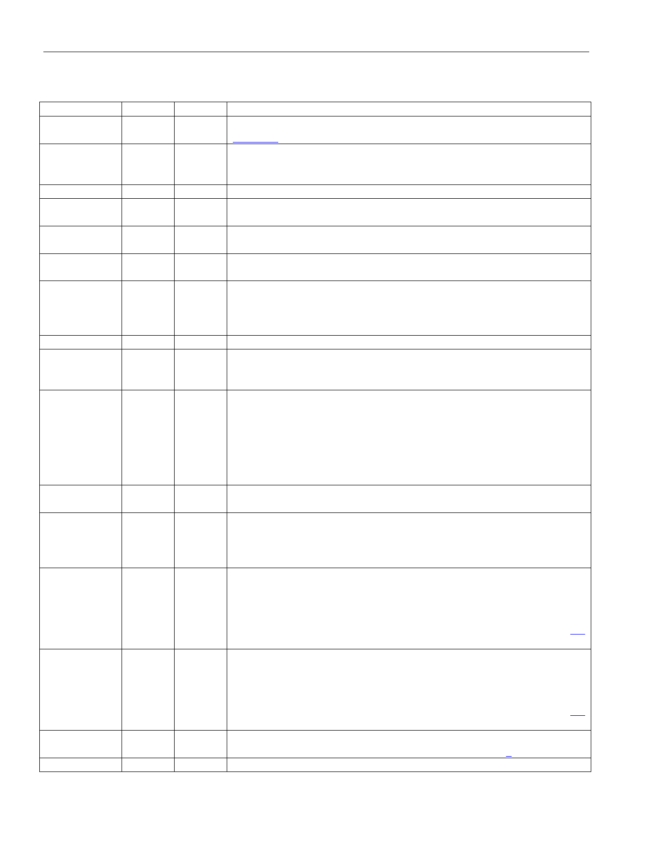
Table 2-5. Pin Descriptions in Serial Port Mode (Sorted by Pin Name,
DS2148T)
NAME
BIS0/BIS1
PIN
32/33
I/O
FUNCTION
I
Bus Interface Select Bits 0 & 1. Used to select bus interface option. See
Table 2-1 for details.
Backplane Clock. A 16.384MHz, 8.192MHz, 4.096MHz, or 2.048MHz
BPCLK
31
O clock output that is referenced to RCLK selectable via CCR5.7 and
CCR5.6. In hardware mode, defaults to 16.384MHz output.
CS
1
I Active-Low Chip Select. Must be low to read or write to the device.
HRST
29
I
Hardware Reset. Bringing HRST low will reset the DS2148 setting all
control bits to their default state of all zeros.
ICES
8
I
Input Clock Edge Select. Selects whether the serial port data input (SDI)
is sampled on rising (ICES =0) or falling edge (ICES = 1) of SCLK.
INT
23
O
Active-Low Interrupt. Flags host controller during conditions and change
of conditions defined in the Status Register. Active low, open drain output.
Master Clock. A 2.048MHz (±50ppm) clock source with TTL levels is
MCLK
30
I
applied at this pin. This clock is used internally for both clock/data
recovery and for jitter attenuation. Use of a T1 1.544MHz clock source is
optional. See Note 1 on clock accuracy at the end of this table.
NA
OCES
PBEO
-
I Not Assigned. Should be tied low.
Output Clock Edge Select. Selects whether the serial port data output
9
I (SDO) is valid on the rising (OCES = 1) or falling edge (OCES = 0) of
SCLK.
PRBS Bit Error Output. The receiver will constantly search for a 215-1
or a 220-1 PRBS depending on the ETS bit setting (CCR1.7). Remains
high if out of synchronization with the PRBS pattern. Goes low when
24
O synchronized to the PRBS pattern. Any errors in the received pattern after
synchronization will cause a positive going pulse (with same period as E1
or T1 clock) synchronous with RCLK. PRBS bit errors can also be
reported to the ECR1 and ECR2 registers by setting CCR6.2 to a logic 1.
RCLK
40
O
Receive Clock. Buffered recovered clock from the line. Synchronous to
MCLK in absence of signal at RTIP and RRING.
RCL/LOTC
25
Receive Carrier Loss/Loss of Transmit Clock. An output which will
O
toggle high during a receive carrier loss (CCR2.7 = 0) or will toggle high
if the TCLK pin has not been toggled for 5 µs ± 2 µs (CCR2.7 = 1).
CCR2.7 defaults to logic 0 when in hardware mode.
RNEG
Receive Negative Data. Updated on the rising edge (CCR2.0 = 0) or the
falling edge (CCR2.0 = 1) of RCLK with the bipolar data out of the line
39
O
interface. Set NRZE (CCR1.6) to a one for NRZ applications. In NRZ
mode, data will be output on RPOS while a received error will cause a
positive-going pulse synchronous with RCLK at RNEG. See Section 6.4
for details.
RPOS
38
RTIP/RRING 27/28
Receive Positive Data. Updated on the rising edge (CCR2.0 = 0) or the
falling edge (CCR2.0 = 1) of RCLK with bipolar data out of the line
O
interface. Set NRZE (CCR1.6) to a one for NRZ applications. In NRZ
mode, data will be output on RPOS while a received error will cause a
positive-going pulse synchronous with RCLK at RNEG. See Section 6.4
for details.
I
Receive Tip and Ring. Analog inputs for clock recovery circuitry. These
pins connect via a 1:1 transformer to the line. See Section 5 for details.
SCLK
5
I Serial Clock. Serial bus clock input.
15 of 73
Share Link: 