DS2148 データシートの表示(PDF) - Maxim Integrated
部品番号
コンポーネント説明
一致するリスト
DS2148 Datasheet PDF : 73 Pages
| |||
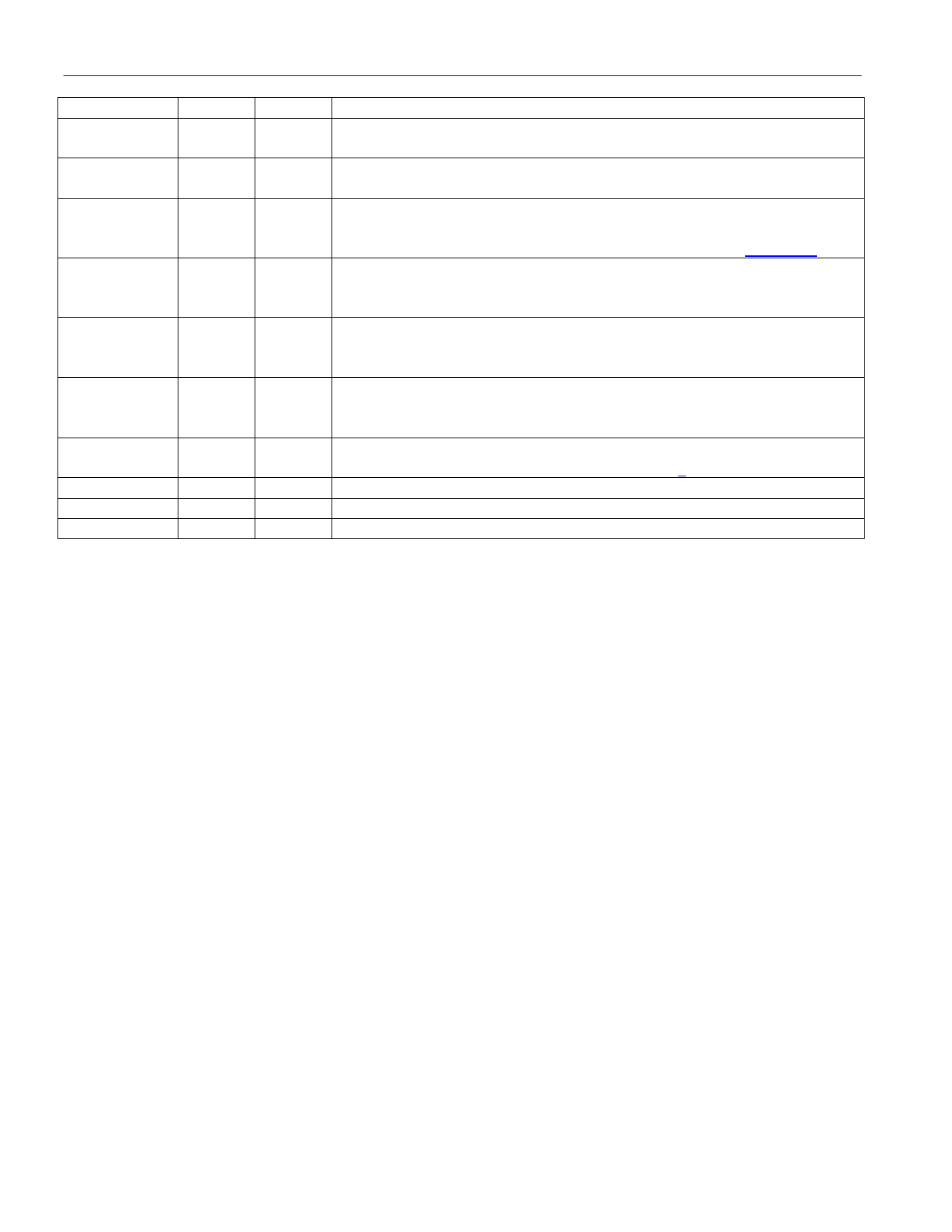
NAME
PIN
SDI
6
SDO
7
TCLK
43
TEST
26
TNEG
42
TPOS
41
TTIP/TRING
VDD
VSM
VSS
34/37
21/36
20
22/35
DS2148/DS21Q48
I/O
FUNCTION
I
Serial Data Input. Sampled on rising edge (ICES = 0) or the falling edge
(ICES = 1) of SCLK.
O
Serial Data Output. Valid on the falling edge (OCES = 0) or the rising
edge (OCES = 1) of SCLK.
Transmit Clock. A 2.048 MHz or 1.544 MHz primary clock. Used to
I clock data through the transmit side formatter. Can be sourced internally
by MCLK or RCLK. See Common Control Register 1 and Figure 1-3.
Tri-State Control. Set high to tri-state all outputs and I/O pins (including
I the parallel control port). Set low for normal operation. Useful in board
level testing.
Transmit Negative Data. Sampled on the falling edge (CCR2.1 = 0) or
I the rising edge (CCR2.1 = 1) of TCLK for data to be transmitted out onto
the line.
Transmit Positive Data. Sampled on the falling edge (CCR2.1 = 0) or the
I rising edge (CCR2.1 = 1) of TCLK for data to be transmitted out onto the
line.
O
Transmit Tip and Ring . Analog line driver outputs. These pins connect
via a step-up transformer to the line. See Section 5 for details.
- 5.0V ±5% Positive Supply
I Voltage Supply Mode. Should be tied high for 5V operation.
- Signal Ground
16 of 73
Share Link: 