DS2148 データシートの表示(PDF) - Maxim Integrated
部品番号
コンポーネント説明
一致するリスト
DS2148 Datasheet PDF : 73 Pages
| |||
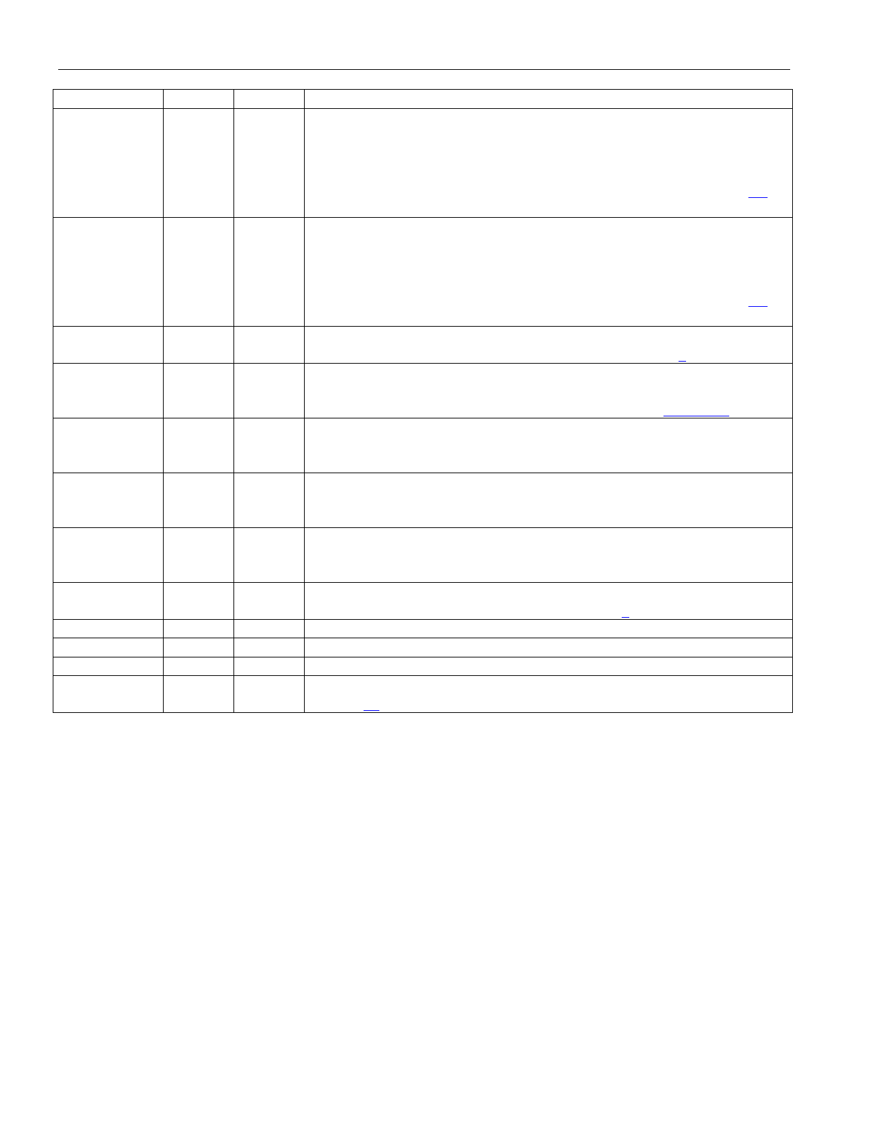
NAME
PIN
RNEG
39
RPOS
38
RTIP/RRING 27/28
TCLK
43
TEST
26
TNEG
42
TPOS
41
TTIP/TRING
VDD
VSM
VSS
WR
(R/W)
34/37
21/36
20
22/35
3
DS2148/DS21Q48
I/O
FUNCTION
Receive Negative Data. Updated on the rising edge (CCR2.0 = 0) or the
falling edge (CCR2.0 = 1) of RCLK with the bipolar data out of the line
O
interface. Set NRZE (CCR1.6) to a one for NRZ applications. In NRZ
mode, data will be output on RPOS while a received error will cause a
positive-going pulse synchronous with RCLK at RNEG. See Section 6.4
for details.
Receive Positive Data. Updated on the rising edge (CCR2.0 = 0) or the
falling edge (CCR2.0 = 1) of RCLK with bipolar data out of the line
O
interface. Set NRZE (CCR1.6) to a one for NRZ applications. In NRZ
mode, data will be output on RPOS while a received error will cause a
positive-going pulse synchronous with RCLK at RNEG. See Section 6.2
for details.
I
Receive Tip and Ring. Analog inputs for clock recovery circuitry. These
pins connect via a 1:1 transformer to the line. See Section 5 for details.
Transmit Clock. A 2.048MHz or 1.544MHz primary clock. Used to clock
I data through the transmit side formatter. Can be sourced internally by
MCLK or RCLK. See Common Control Register 1 and Figure 1-3.
Tri-state Control. Set high to tri-state all outputs and I/O pins (including
I the parallel control port). Set low for normal operation. Useful in board
level testing.
Transmit Negative Data. Sampled on the falling edge (CCR2.1 = 0) or
I the rising edge (CCR2.1 = 1) of TCLK for data to be transmitted out onto
the line.
Transmit Positive Data. Sampled on the falling edge (CCR2.1 = 0) or the
I rising edge (CCR2.1 = 1) of TCLK for data to be transmitted out onto the
line.
O
Transmit Tip and Ring. Analog line driver outputs. These pins connect
via a step-up transformer to the line. See Section 5 for details.
- 5.0V ±5% Positive Supply
I Voltage Supply Mode. Should be tied high for 5V operation
- Signal Ground
I
Active-Low Write Input (Read/Write). See the bus timing diagrams in
Section 10.
13 of 73
Share Link: 