VT82C596 データシートの表示(PDF) - Unspecified
部品番号
コンポーネント説明
一致するリスト
VT82C596 Datasheet PDF : 96 Pages
| |||
:H &RQQHFW 7HFKQRORJLHV ,QF
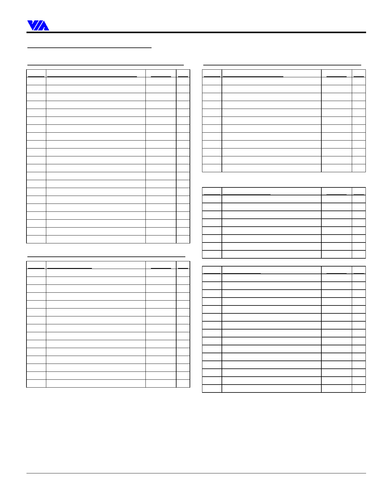
PCI Function 0 Registers - PCI-to-ISA Bridge
Configuration Space PCI-to-ISA Bridge Header Registers
Offset PCI Configuration Space Header
1-0 Vendor ID
3-2 Device ID
5-4 Command
7-6 Status
8 Revision ID
9 Programming Interface
A Sub Class Code
B Base Class Code
C -reserved- (cache line size)
D -reserved- (latency timer)
E Header Type
F Built In Self Test (BIST)
10-27 -reserved- (base address registers)
28-2B -reserved- (unassigned)
2F-2C Subsystem ID Read
30-33 -reserved- (expan. ROM base addr)
34-3B -reserved- (unassigned)
3C -reserved- (interrupt line)
3D -reserved- (interrupt pin)
3E -reserved- (min gnt)
3F -reserved- (max lat)
Default Acc
1106 RO
0596 RO
0087 RW
0200 WC
nn RO
00 RO
01 RO
06 RO
00 —
00 —
80 RO
00 RO
00 —
00 —
00 RO
00 —
00 —
00 —
00 —
00 —
00 —
Configuration Space PCI-to-ISA Bridge-Specific Registers
Offset ISA Bus Control
Default Acc
40 ISA Bus Control
00 RW
41 ISA Test Mode
00 RW
42 ISA Clock Control
00 RW
43 ROM Decode Control
00 RW
44 Keyboard Controller Control
00 RW
45 Type F DMA Control
00 RW
46 Miscellaneous Control 1
00 RW
47 Miscellaneous Control 2
00 RW
48 Miscellaneous Control 3
01 RW
49 -reserved-
00 —
4A IDE Interrupt Routing
04 RW
4B -reserved-
00 —
4C DMA / Master Mem Access Control 1 00 RW
4D DMA / Master Mem Access Control 2 00 RW
4F-4E DMA / Master Mem Access Control 3 0300 RW
VT82C596B
Configuration Space PCI-to-ISA Bridge-Specific Registers
Offset Plug and Play Control
Default Acc
50 -reserved- (do not program)
24 RW
51-53 -reserved-
00 —
54 PCI IRQ Edge / Level Selection
00 RW
55 PnP Routing for External MIRQ0-1
00 RW
56 PnP Routing for PCI INTB-A
00 RW
57 PnP Routing for PCI INTD-C
00 RW
58 PnP Routing for External MIRQ2
00 RW
59 PIRQ Pin Configuration
04 RW
5A KBC / RTC Control
x4† RW
5B Internal RTC Test Mode
00 RW
5C DMA Control
00 RW
5F-5D -reserved-
00 —
† Bit 7-4 power-up default value depends on external strapping
Offset Distributed DMA
61-60 Channel 0 Base Address / Enable
63-62 Channel 1 Base Address / Enable
65-64 Channel 2 Base Address / Enable
67-66 Channel 3 Base Address / Enable
69-68 Serial IRQ Control
6B-6A Channel 5 Base Address / Enable
6D-6C Channel 6 Base Address / Enable
6F-6E Channel 7 Base Address / Enable
Default Acc
0000 RW
0000 RW
0000 RW
0000 RW
0000 RW
0000 RW
0000 RW
0000 RW
Offset Miscellaneous
70 Subsystem ID Write
71-73 -reserved-
77-74 GPIO / Chip Select Control
7B-78 Programmable Chip Select Control
7F-7C PC/PCI Control
80 Programmable Chip Select Mask
81 ISA Positive Decoding Control 1
82 ISA Positive Decoding Control 2
83 ISA Positive Decoding Control 3
84 ISA Positive Decoding Control 4
85-86 -reserved-
87 Test 1
88 Test 2
89 PLL Control
8A-FF -reserved-
Default Acc
00 WO
00 —
0000 0000 RW
0000 0000 RW
0000 0000 RW
00 RW
00 RW
00 RW
00 RW
00 RW
00 —
00 RW
00 RW
00 RW
00 —
Revision 0.3 June 17, 1999
-23-
Register Overview
Share Link: 