VT82C596 データシートの表示(PDF) - Unspecified
部品番号
コンポーネント説明
一致するリスト
VT82C596 Datasheet PDF : 96 Pages
| |||
:H &RQQHFW 7HFKQRORJLHV ,QF
VT82C596B
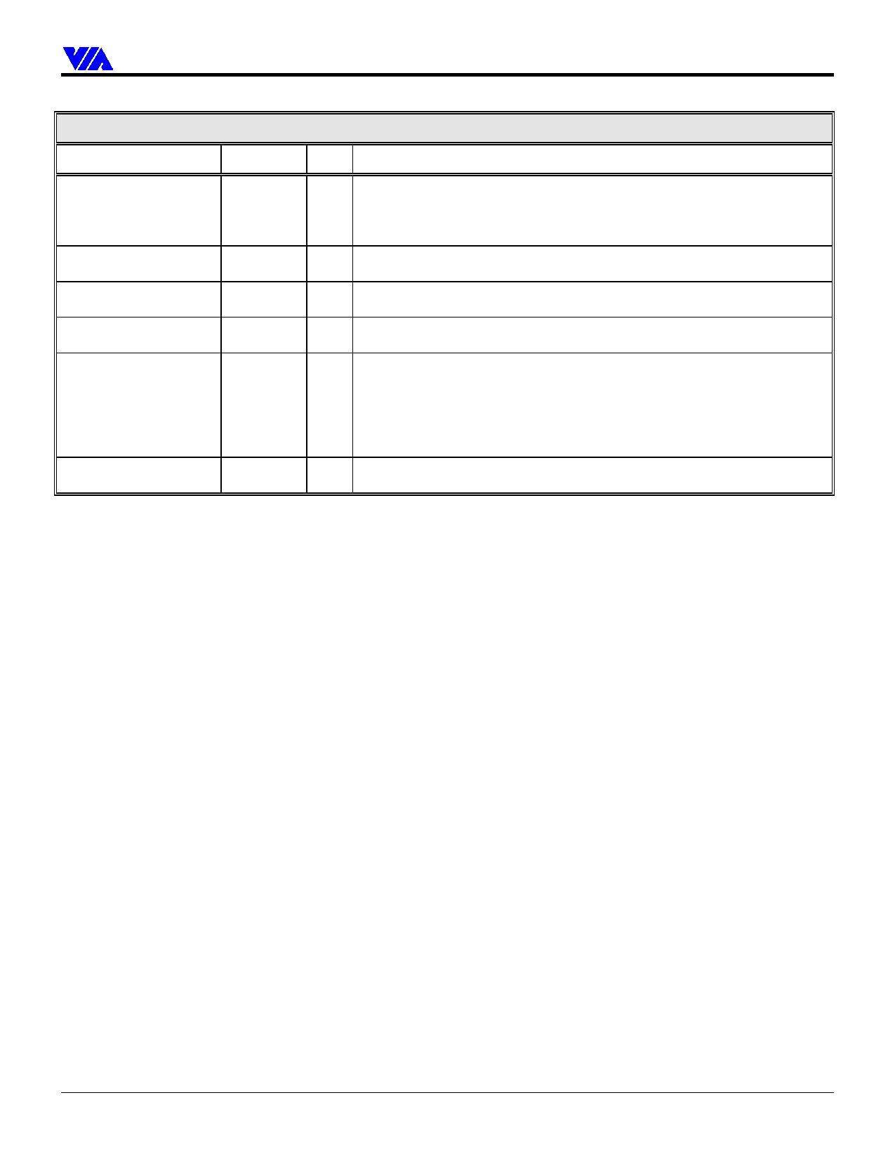
Signal Name
PWRBTN#
SLPBTN# / GPI13
RCIN#
RSMRST#
EXTSMI#
PCIREQ[A-D]#
Pin #
U20
L2
N20
M17
V20
E10, A11,
B11, C11
Power Management
I/O Signal Description
I Power Button. Used by the Power Management subsystem to monitor an
external system on/off button or switch. The VT82C596B performs a 200us
debounce of this input if Rx40[5] is set to 1. This input is referenced to
VCCSUS.
I ACPI Sleep Button. General purpose input 13, but also functions as the ACPI
sleep button if bit-9 of register 0 of ACPI I/O Space (Function 3) is enabled.
I Reset CPU. This signal from an optional external keyboard controller (if
used) causes an INIT signal to be generated to the CPU.
I Resume Reset. Resets the internal logic connected to the VCCSUS power
plane and also resets portions of the internal RTC logic.
IOD External System Management Interrupt. When enabled to allow it, a falling
edge on this input causes an SMI# to be generated to the CPU to enter SMI
mode. Once asserted, this pin should be held low for at least four PCICLKs.
The VT82C596B also asserts EXTSMI# in response to SMI# being activated
within the Serial IRQ function. This pin should be connected to an external
pullup.
I Power Management PCI Requests. Used by internal power management to
monitor PCI requests for use of the PCI bus.
Revision 0.3 June 17, 1999
-18-
Pinouts
Share Link: 