V370PDC データシートの表示(PDF) - QuickLogic Corporation
部品番号
コンポーネント説明
一致するリスト
V370PDC
QuickLogic Corporation

V370PDC Datasheet PDF : 14 Pages
| |||
V370PDC
3.0 DC Specifications
The DC specifications for the PCI bus signals match exactly those given in the PCI Specification, Rev.
2.2 Section 4.2.1.1. For more information on the PCI DC specifications, see the PCI Specification.
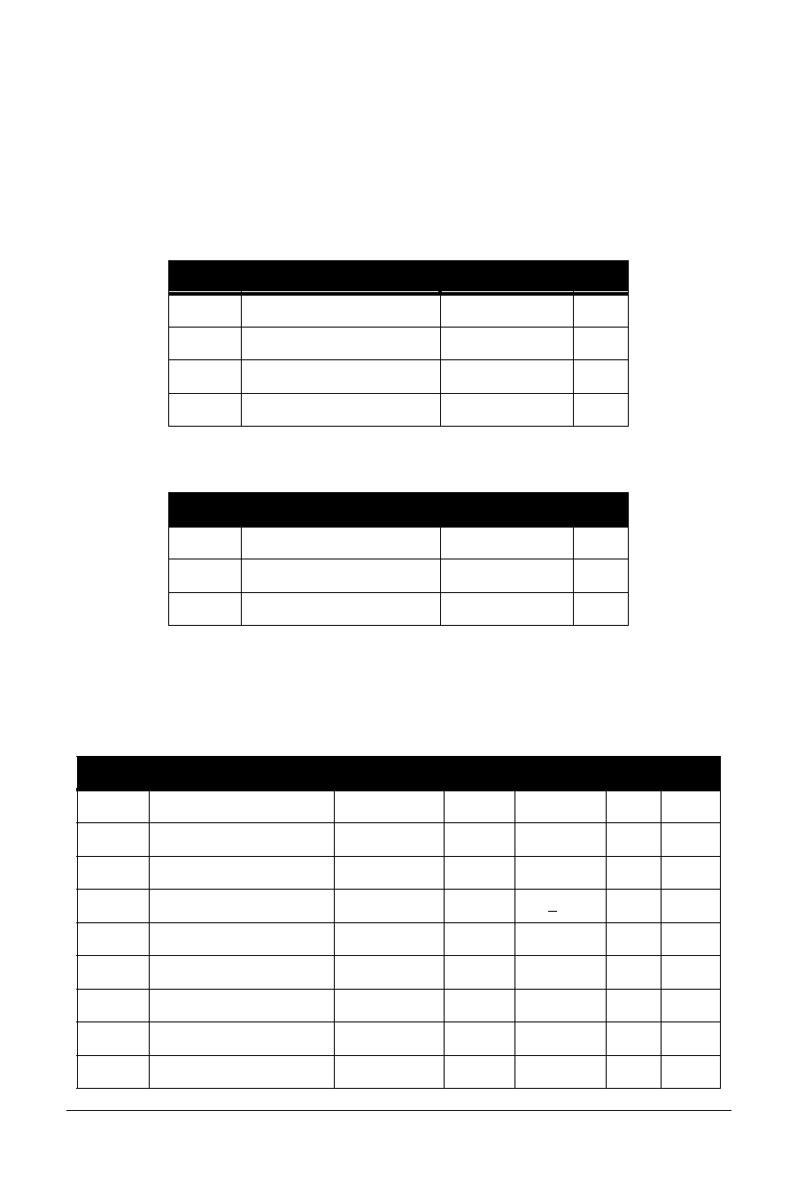
Table 5: Absolute Maximum Ratings
Symbol
Parameter
VCC
VIN
IOUT
TSTG
Supply voltage
DC input voltage
DC output current
Storage temperature range
Value
-0.3 to +3.6
-0.3 to 6.0
TBA
-55 to +125
Units
V
V
mA
°C
Table 6: Guaranteed Operating Conditions
Symbol
Parameter
VCC Supply voltage
Theta Ja Thermal resistance
TA Ambient temperature range
Value
3.0 to 3.6
TBA
-40 to +85
Units
V
°C/w
°C
3.1 PCI Bus DC Specifications
Table 7: PCI Bus Signals DC Operating Specifications
Symbol
Parameter
Condition
Min
VIH Input high voltage
0.5VCC
VIL Input low voltage
-0.5
IIH Input high leakage current
0.7VCC
IIL Input low leakage current 0 < VIN < VCC
VOH Output high voltage
IOUT = -500µA 0.9VCC
VOL Output low voltage
IOUT = 1500µA
CIN Input pin capacitance
CCLK PCLK pin capacitance
5
CIDSEL IDSEL pin capacitance
Max
Units Notes
VCC + 0.5
V
0.3VCC
V
µA
1
+10
µA
1
V
0.1VCC
V
2
10
pF
3
12
pF
8
pF
4
Copyright © 1999, V3 Semiconductor Corp.
V370PDC_A0 Data Sheet Rev 1.00 DS-PD01-0100
9
Share Link: