V370PDC データシートの表示(PDF) - QuickLogic Corporation
部品番号
コンポーネント説明
一致するリスト
V370PDC
QuickLogic Corporation

V370PDC Datasheet PDF : 14 Pages
| |||
V370PDC
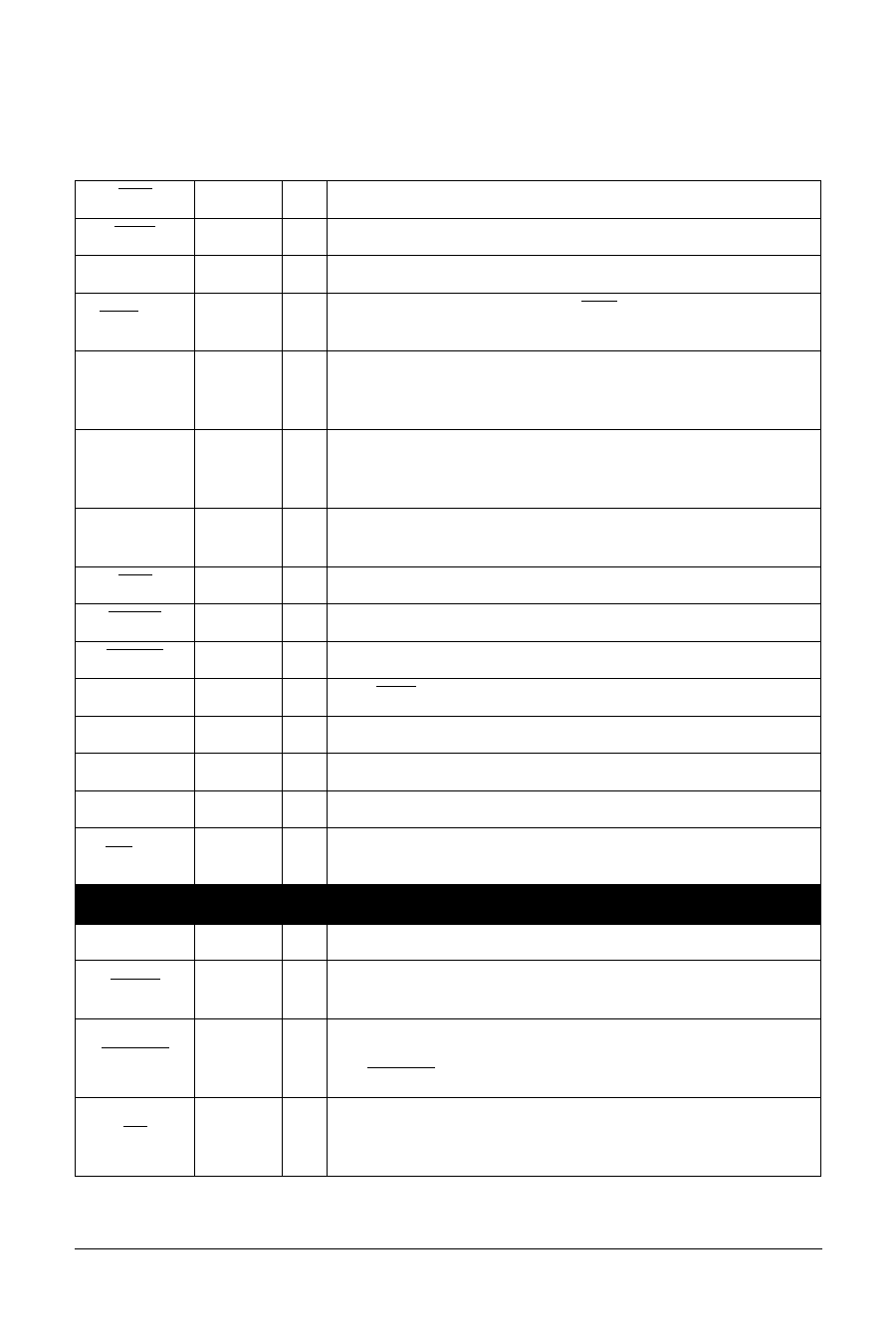
CAS
MWE
MAD[31:0]
DQM[3:0]
MARB_IN
MARB_OUT
ALE
ADS
BLAST
READY
WNR
SDA
SCL
IOC[11:0]
INT[3:0]
Signal
RSTIN
RSTOUT
CH
Table 3: Signal Descriptions (cont’d)
O12
O12
I/O8
O8
I
O8
O8
O8
O8
I
O8
I/OD
O2
I/O8
I/O8
Type
I
O8
I
Z SDRAM Column Address Strobe
Z SDRAM Memory Write Enable
Z SDRAM and peripheral bus data
Z
SDRAM Data Mask (these act as MBE[3:0], A[1:0] for peripheral
access)
Peripheral bus arbitration input: Treated as bus request input
when V370PDC is the primary bus master. When V370PDC is the
secondary bus master, this input acts as bus grant.
Peripheral bus arbitration output: Treated as bus grant output
0 when V370PDC is the primary bus master. When V370PDC is the
secondary bus master, this output acts bus request.
Z
Address Latch Enable: used to latch the address on MAD[31:0]
during the address phase of a peripheral bus access.
Z Asserted low to indicate the beginning of a bus cycle.
Z Burst last.
Data ready.
Z Write/Read.
Z Serial EEPROM Data
Z Serial EEPROM Clock
Z Multi-purpose I/O that can be configured for many functions
Z
General purpose interrupt inputs/outputs: may be used for either
PCI or local processor interrupts
Mode and Reset
R
Description
Reset Input: Active low reset input used to initialize all internal
functions of the chip.
Reset Output: Driven active when the input reset is driven active.
0 Driven inactive when the RSTOUT bit in the system register is set.
The RSTOUT signal is synchronous to the rising edge of CLKIN.
PCI Precharge Bias: This signal is driven low to activate the on-
chip precharge bias for use in PICMG Hot Swap applications.
Non-Hot Swap applications should pull this signal high.
4
V370PDC_A0 Data Sheet Rev 1.00 DS-PD01-0100
Copyright © 1999, V3 Semiconductor Inc.
Share Link: