V370PDC データシートの表示(PDF) - QuickLogic Corporation
部品番号
コンポーネント説明
一致するリスト
V370PDC
QuickLogic Corporation

V370PDC Datasheet PDF : 14 Pages
| |||
V370PDC
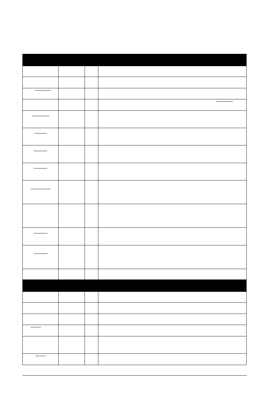
Signal
AD[31:0]
C/BE[3:0]
PAR
FRAME
IRDY
TRDY
STOP
DEVSEL
IDSEL
PERR
SERR
PCLK
Signal
CLKIN
CLKOUT
DCS[3:0]
MA[14:0]
RAS
Table 3: Signal Descriptions
Type Ra
PCI Bus Interface
Description
PCI I/O Z Address and data, multiplexed on the same pins.
PCI I
Bus Command and Byte Enables, multiplexed on the same pins.
PCI I/O Z Parity represents even parity across AD[31:0] and C/BE[3:0].
PCI I
Cycle Frame indicates the beginning and burst length of an
access.
PCI I
Initiator Ready indicates the initiating agent’s (bus master’s) ability
to complete the current data phase of the transaction.
PCI O
Z
Target Ready indicates the target agent’s (selected device’s) abil-
ity to complete the current data phase of the transaction.
PCI O
Z
Stop indicates the current target is requesting the master to stop
the current transaction (retry or disconnect).
PCI O
Device Select, when actively driven by a target, indicates the driv-
Z ing device has decoded its address as the target of the current
access.
PCI I
Initialization Device Select is used as a chip select during configu-
ration read and write transactions. It must be driven high in orde
to access the chip’s internal configuration space.
PCI I/O
Z
Parity Error is used to report data parity errors during all PCI
transactions except a Special Cycle.
System Error is used to report address parity errors, data parity
PCI I/OD Z errors on the Special Cycle command, or any other system error
where the result will be catastrophic.
PCI I
PCLK provides timing for all transactions on the PCI bus.
SDRAM and Peripheral Bus Interface
Type R
Description
I
Local clock input
O12
X Buffered PCI clock output
O8
Z SDRAM Chip Select
O12
Z
SDRAM Memory Address (also, A[16:2] for peripheral access).
MA[14:13] are typically used for BA[1:0]
O12
Z SDRAM Row Address Strobe
Copyright © 1999, V3 Semiconductor Corp.
V370PDC_A0 Data Sheet Rev 1.00 DS-PD01-0100
3
Share Link: