V370PDC データシートの表示(PDF) - QuickLogic Corporation
部品番号
コンポーネント説明
一致するリスト
V370PDC
QuickLogic Corporation

V370PDC Datasheet PDF : 14 Pages
| |||
V370PDC
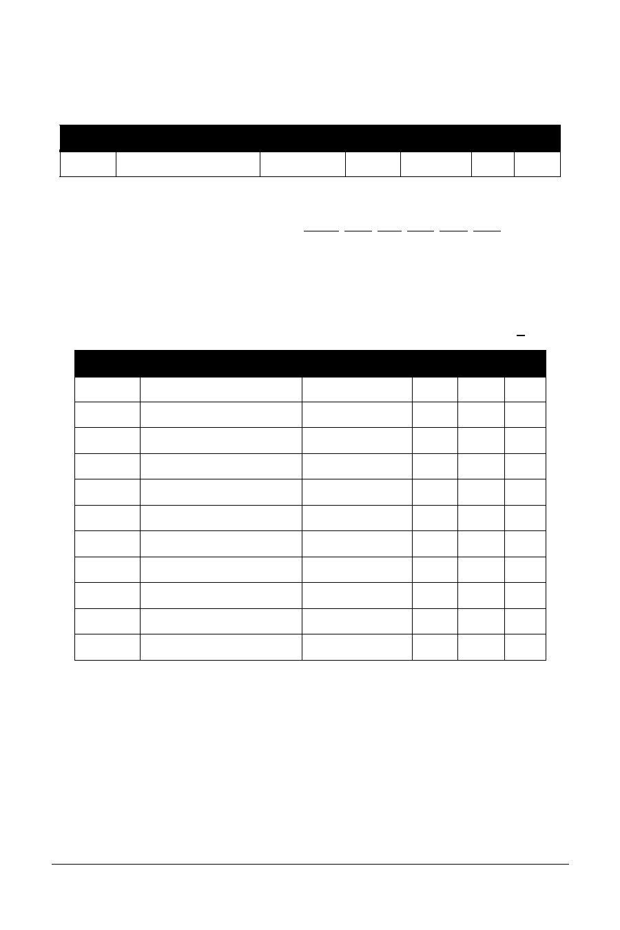
Table 7: PCI Bus Signals DC Operating Specifications
Symbol
Parameter
Condition
Min
Max
Units Notes
LPIN Pin inductance
20
nH
Notes:
1. Input leakage currents include high impedance output leakage for all bi-directional buffers with tri-state out-
puts.
2. Signals without pull-up resistors have greater than 3mA low output current. Signals requiring pull resistors
have greater than 6mA output current. The latter include FRAME, TRDY, IRDY, STOP, SERR, PERR.
3. Absolute maximum pin capacitance for a PCI unit is 10pF (except for CLK).
4. Lower capacitance on this input-only pin allows for non-resistive coupling to AD[xx].
3.2 Local Bus DC Specification
Table 8: Local Bus Signals DC Operating Specifications (VCC = 3.3V+ 0.3V)
Symbol
Parameter
Condition
Min
VIH
Input high voltage
2.0
VIL
Input low voltage
IIH
Input high leakage current
VIN = VCC
-10
IIL
Input low leakage current
VIN=GND
-10
VOH Output high voltage
IOUT = -2, -8, -12mA 2.4
VOL Output low voltage
IOUT = 2, 8, 12mA
IOZL Low level float input leakage
VOL = GND
-10
IOZH High level float input leakage
VOH = VCC
-10
ICC (max) Maximum supply current
ICC (typ) Typical supply current
CIO
Input and output capacitance
Max Units
V
0.8
V
10
µA
10
µA
V
0.4
V
10
µA
10
µA
TBA mA
TBA mA
TBA pF
10
V370PDC_A0 Data Sheet Rev 1.00 DS-PD01-0100
Copyright © 1999, V3 Semiconductor Inc.
Share Link: