V370PDC データシートの表示(PDF) - QuickLogic Corporation
部品番号
コンポーネント説明
一致するリスト
V370PDC
QuickLogic Corporation

V370PDC Datasheet PDF : 14 Pages
| |||
V370PDC Rev. A0
High Performance PCI SDRAM Controller with
Integrated Peripheral Control Unit
• Fully compliant with PCI 2.2 specification target
interface
• Multiplexed or Non-multiplexed 8-, 16-, or 32-bit
generic peripheral bus interface
• Support up to 1 Gbyte of SDRA
• Support up to 2 single banks or 1 dual bank
industrial standard 168-pin PC SDRAM DIMM
• Support up to 1Kbyte of burst access from PCI
• Up to 5 programmable chip select for peripheral
strobe generation
• Large On-Chip FIFOs using V3’s unique
DYNAMIC BANDWIDTH ALLOCATION™
architectu e
• Buffered PCI clock output
• Hot Swap Ready (PICMG™ Hot Swap
Specification)
• Implementation of PCI Bus Power Management
Interface Specification Version 1.0
• Initialization through PCI or serial EEPRO
• Programmable PCI and local interrupt
management
• Two 32-bit General Purpose Timers
• Up to 66 MHz local bus clock with asynchronous
PCI clock up to 33MHz
• 3.3V operation with 5V tolerant inputs
• Industrial Temperature Range (-40C to +85C)
• Low cost 160-pin PQFP package
The V370PDC PCI SDRAM Controller simplifies the
design of PCI based memory sub-systems. System
designers can replace many lower integration support
components wit this single, high-integration device
saving design time, board area, and manufacturing
cost.
The V370PDC from V3 Semiconductor is a high
performance PCI SDRAM Controller with integrated
peripheral control unit o perating at up to 66 MHz local
bus speed. It features multiple address translation
units from PCI which allow designers the freedom to
customize their local address space. Access latency of
slower peripherals are absorbed through the large On-
Chip FIFOs.
The peripheral bus provides low latency access t
SDRAM. The peripheral control unit on the V370PDC
also performs address decoding and chip-select
strobes generation for SRAM, PROM and other slow
peripherals. The peripheral bus can also be tri-stated
through a simple hand-shaking protocol to allow other
local bus masters control of the bus.
The SDRAM Controller connects the PCI bus through
on-chip FIFOs to SDRAM arrays of up to 1 Gbytes in
size. The fully programmable SDRAM controller also
supports the use of Enhanced SDRAM to achiev
even greater performance. Burst accesses of up to 1
Kbyte from PCI is supported.
The two general purpose 32-bit timers can be
individually configured as a pulse width modulator, or
used in other modes such as retriggerable or one-
shot. Interrupts for a real time OS can be easily
generated by the system heartbeat timer. A watchdog
timer is also provided for graceful recovery from
catastrophic program failures. Interrupt requests for all
on-chip peripherals are managed by the Interrupt
Control Unit. Additionally, off-chip interrupts can b
routed to the Interrupt Control Unit.
The V370PDC is packaged in a low-cost 160-pin EIJA
Plastic Quad Flat Pack (PQFP), and is available i
66MHz speed grade.
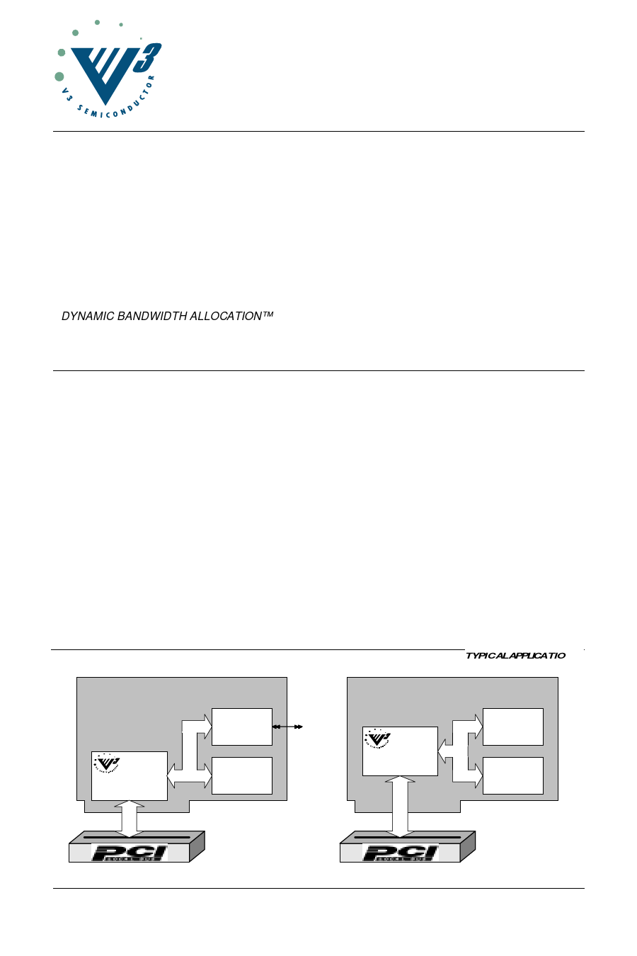
TYPICALAPPLICATIO
PCI-to-ISA Conversion
Application
V370PDC
ISA
Conversion
Logic
SDRAM
and PROM
PCI Target Only
Application
V370PDC
SRAM/
FLASH
SDRAM
Copyright © 1999, V3 Semiconductor Corp.
V370PDC_A0 Data Sheet Rev 1.00 DS-PD01-0100
1
V3 Semiconductor reserves the right to change the specifications of this product without notice.
V370PDC is a trademark of V3 Semiconductor Inc. All other trademarks are the property of their respective owners.
Share Link: