UPD72862 データシートの表示(PDF) - NEC => Renesas Technology
部品番号
コンポーネント説明
一致するリスト
UPD72862 Datasheet PDF : 36 Pages
| |||
µPD72862
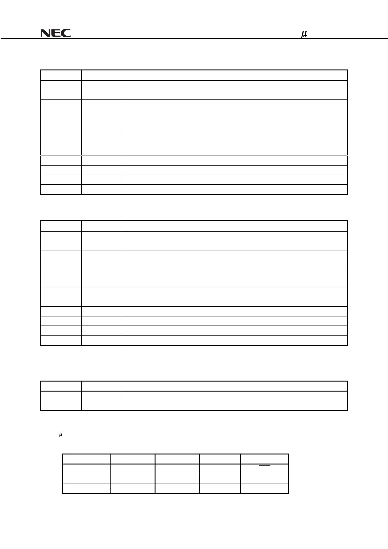
(3) Function Reset Status Register (FRSR) ( Base Address 1 ( 2 )+ 8H )
Bits
0
1
2
3
4
14-5
15
31-16
R/W
Description
R
Write Protect (No Use).
Read only as ‘0’
R
Ready Status (No Use).
Read only as ‘0’
R
Battery Voltage Detect 2 (No Use).
Read only as ‘0’
R
Battery Voltage Detect 1 (No Use).
Read only as ‘0’
R/W
General Wakeup Mask
R
Reserved. Read only as ‘0’
R/W
Interrupt
R
Reserved. Read only as ‘0’
(4) Function Force Event Register (FFER) ( Base Address 1 ( 2 )+ CH )
Bits
0
1
2
3
4
14-5
15
31-16
R/W
Description
R
Write Protect (No Use).
Read only as ‘0’
R
Ready Status (No Use).
Read only as ‘0’
R
Battery Voltage Detect 2 (No Use).
Read only as ‘0’
R
Battery Voltage Detect 1 (No Use).
Read only as ‘0’
R/W
General Wakeup Mask
-
No Use
R/W
Interrupt
R
Reserved. Read only as ‘0’
2.2.2 Offset_28 Cardbus CIS Pointer
This register specifies start memory address of the Cardbus CIS Area.
Bits
31-0
R/W
R
Starting Pointer of CIS Area.
Constant value of 00000080H.
Description
2.2.3 Offset_80 CIS Area
The µPD72862 supports external Serial ROM(AT24C02 compatible) interface.
CIS Area Register can be loaded from external Serial ROM in the CIS area when CARD_ON are HIGH.
CARD_ON
0
0
1
CIS_ON
1
0
X
Bus
PCI
PCI
Cardbus
CIS
OFF
ON
ON
FUNCTION
PME
CSTSCHG
CSTSCHG
20
Data Sheet S14265EJ2V0DS00
Share Link: 