UPD72862 データシートの表示(PDF) - NEC => Renesas Technology
部品番号
コンポーネント説明
一致するリスト
UPD72862 Datasheet PDF : 36 Pages
| |||
µPD72862
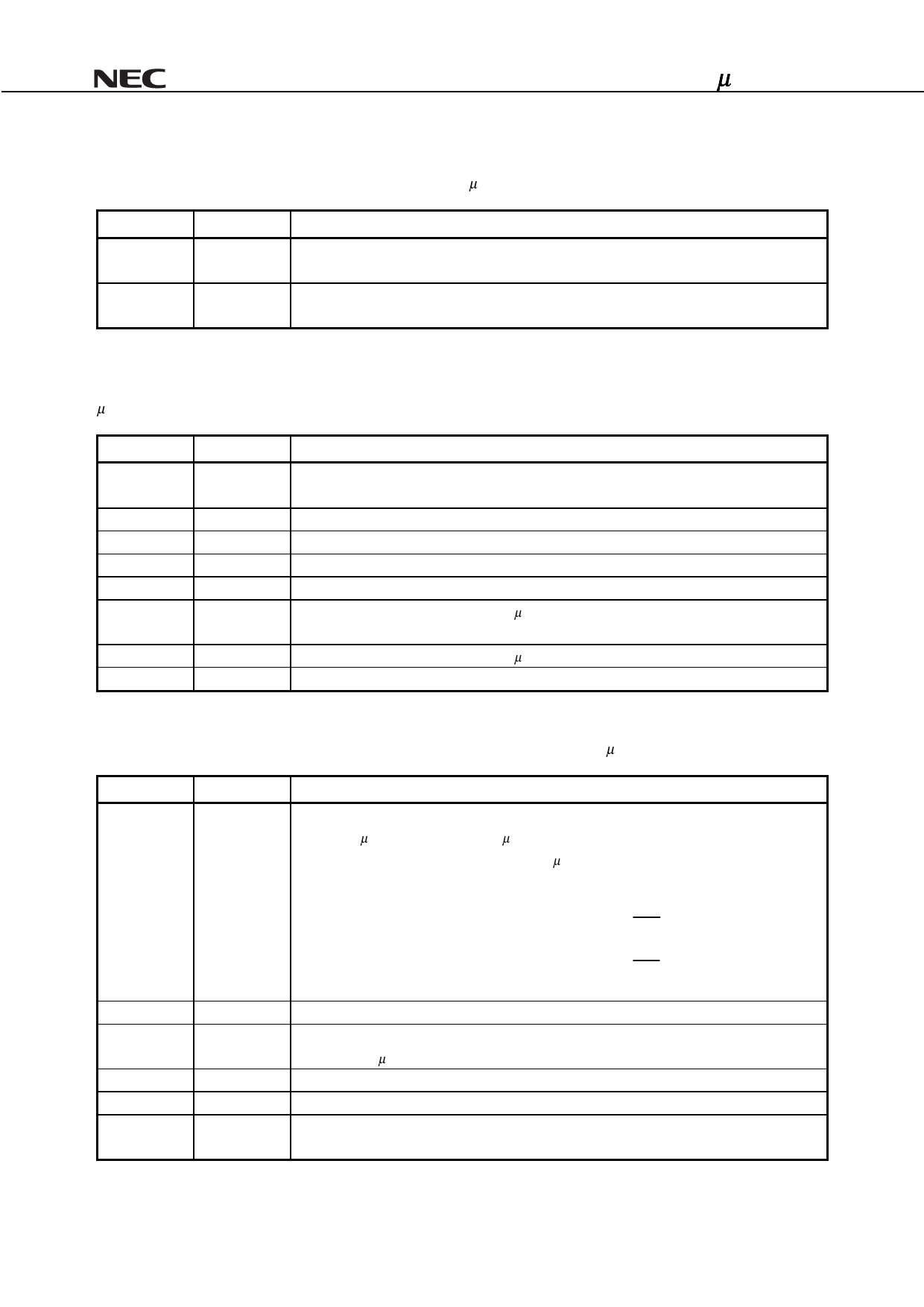
2.1.21 Offset_60 Cap_ID & Next_Item_Ptr Register
The Cap_ID signals that this item in the Linked List is the registers defined for PCI Power Management, while the
Next_Item_Ptr describes the location of the next item in the µPD72862’s Capability List.
Bits
7-0
15-8
R/W
Description
R
Cap_ID Constant value of 01H. The default value identified the Link List item as being the PCI
Power Management registers, while the ID value is assigned by the PCI SIG.
R
Next_Item_Ptr Constant value of 00H. It indicated that there are no more items in the Link
List.
2.1.22 Offset_62 Power Management Capabilities Register
This is a 16-bit read-only register that provides information on the power management capabilities of the
µPD72862.
Bits
2-0
3
4
5
8,6
9
10
15-11
R/W
Description
R
version Constant value of 001. The power management registers are implemented as defined
in revision 1.0 of PCI Bus Power Management Interface Specification.
R
PME clock Constant value of 0.
R
Auxiliary power source Constant value of 0. The alternative power source is not supported.
R
DIS Constant value of 0.
R
Reserved Constant value of 000.
R
D1_support Constant value of 0. The µPD72862 does not support the D1 Power
Management state.
R
D2_support Constant value of 1. The µPD72862 supports the D2 Power Management state.
R
PME_support Constant value of 01100.
2.1.23 Offset_64 Power Management Control/Status Register
This is a 16-bit read-only register that provides control status information of the µPD72862.
Bits
1,0
7-2
8
12-9
14,13
15
R/W
Description
R/W
PowerState Default value is undefined. This field is used both to determine the current power
state of the µPD72862 and to set the µPD72862 into a new power state. As D1 is not
supported in the current implementation of the µPD72862, writing of ‘01’ will be ignored.
00: D0 (DMA contexts: ON, Link Layer: ON)
01: Reserved (D1 state not supported)
10: D2 (DMA contexts: OFF, Link Layer: OFF, LPS: OFF, PME will be asserted upon
LinkON being active)
11: D3 (DMA contexts: OFF, Link Layer: OFF, LPS: OFF, PME will be asserted upon
LinkON being active, Power can be removed)
R
Reserved Constant value of 000000.
R/W
PME_En Default value of 0. This field is used to enable the specific power management
features of the µPD72862.
R
Data_Select Constant value of 0000.
R
Data_Scale Constant value of 00.
R/W
PME_Status Default value is undefined. A write of ‘1’ clears this bit, while a write of ‘0’ is
ignored.
Data Sheet S14265EJ2V0DS00
17
Share Link: 