DS21448 データシートの表示(PDF) - Dallas Semiconductor -> Maxim Integrated
部品番号
コンポーネント説明
一致するリスト
DS21448 Datasheet PDF : 60 Pages
| |||
DS21448 3.3V T1/E1/J1 Quad Line Interface
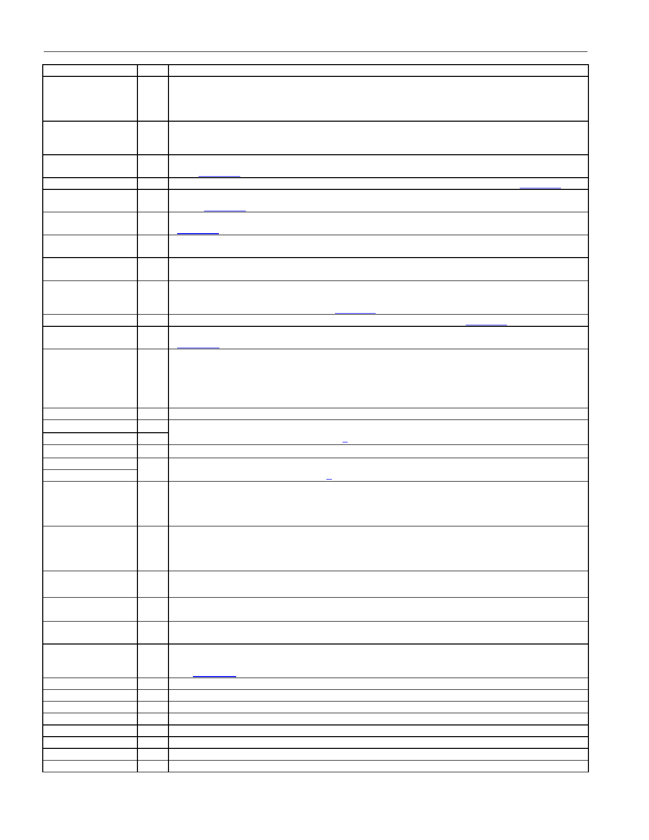
PIN
CES
TPD
TX0/TX1
LOOP0/LOOP1
MM0/MM1
RT1/RT0
TEST
HRST
MCLK
BIS0/BIS1
EGL1–EGL4
PBEO1–PBEO4
RCL1–RCL4
RTIP1–RTIP4
RRING1–RRING4
BPCLK1–BPCLK4
TTIP1–TTIP4
TRING1–TRING4
RPOS1–RPOS4
RNEG1–RNEG4
RCLK1–RCLK4
TPOS1–TPOS4
TNEG1–TNEG4
TCLK1–TCLK4
JTRST
JTMS
JTCLK
JTDI
JTDO
VSM
TVDD1–TVDD4
VDD1–VDD4
I/O
FUNCTION
Receive and Transmit Clock Select. Selects which RCLK edge to update RPOS and RNEG and
I
which TCLK edge to sample TPOS and TNEG. CES combines TCES and RCES.
0 = update RPOS/RNEG on rising edge of RCLK; sample TPOS/TNEG on falling edge of TCLK
1 = update RPOS/RNEG on falling edge of RCLK; sample TPOS/TNEG on rising edge of TCLK
Transmit Power-Down
I 0 = normal transmitter operation
1 = powers down the transmitter and tri-states TTIP and TRING pins
I
Transmit Data Source Select Bits 0 and 1. These inputs determine the source of the transmit
data (Table 4-B).
I Loopback Select Bits 0 and 1. These inputs determine the active loopback mode (Table 4-A).
I
Monitor Mode Select Bits 0 and 1. These inputs determine if the receive equalizer is in a monitor
mode (Table 4-D).
I
Receive LIU Termination Select Bits 0 and 1. These inputs determine the receive termination
(Table 4-E).
I
Tri-State Control. Set high to tri-state all outputs and I/O pins (including the parallel control port).
Set low for normal operation. Useful in board-level testing.
I
Hardware Reset. Bringing HRST low resets the DS21448, setting all control bits to the all-zero
default state.
Master Clock. A 2.048MHz (±50ppm) clock source with TTL levels is applied at this pin. This
I clock is used internally for both clock/data recovery and for jitter attenuation. A T1 1.544MHz
clock source is optional (Note 1). See Table 4-F for details.
I Bus Interface Select Bit 0 and 1. Used to select bus interface option (Table 2-A).
I
Receive Equalizer Gain-Limit Select. These bits control the sensitivity of the receive equalizers
(Table 4-C).
PRBS Bit-Error Output. The receiver constantly searches for a 215 - 1 PRBS (ETS = 0) or a
QRSS PRBS (ETS = 1). The pattern is chosen automatically by the value of the ETS pin. It
O remains high if it is out of synchronization with the PRBS pattern. It goes low when synchronized
to the PRBS pattern. Any errors in the received pattern after synchronization cause a positive-
going pulse (with same period as E1 or T1 clock) synchronous with RCLK.
O Receive Carrier Loss. An output that toggles high during a receive carrier loss.
I Receive Tip and Ring. Analog inputs for clock recovery circuitry. These pins connect through a
I 1:1 transformer to the line. See Section 7 for details.
O Backplane Clock. A 16.384MHz clock output that is referenced to RCLK.
O
Transmit Tip and Ring. Analog line-driver outputs. These pins connect through a step-up
transformer to the line. See Section 7 for details.
Receive Positive Data. Updated on the rising edge (CES = 0) or the falling edge (CES = 1) of
O
RCLK with bipolar data out of the line interface. In NRZ mode (NRZE = 1), data is output on
RPOS, and a received error (BPV, CV, or EXZ) causes a positive-going pulse synchronous with
RCLK at RNEG.
Receive Negative Data. Updated on the rising edge (CES = 0) or the falling edge (CES = 1) of
O
RCLK with bipolar data out of the line interface. In NRZ mode (NRZE = 1), data is output on
RPOS, and a received error (BPV, CV, or EXZ) causes a positive-going pulse synchronous with
RCLK at RNEG.
O
Receive Clock. Buffered recovered clock from the line. Synchronous to MCLK in absence of
signal at RTIP and RRING.
I
Transmit Positive Data. Sampled on the falling edge (CES = 0) or the rising edge (CES = 1) of
TCLK for data to be transmitted out onto the line.
I
Transmit Negative Data. Sampled on the falling edge (CES = 0) or the rising edge (CES = 1) of
TCLK for data to be transmitted out onto the line.
Transmit Clock. A 2.048MHz or 1.544MHz primary clock used to clock data through the transmit
I side formatter. It can be sourced internally by MCLK or RCLK. See Common Control Register 1
and Figure 1-3.
I JTAG Reset
I JTAG Mode Select
I JTAG Clock
I JTAG Data In
O JTAG Data Out
I Voltage Supply Mode (LQFP only). VSM should be wired low for correct operation.
– 3.3V, ±5% Transmitter Positive Supply
— 3.3V, ±5% Positive Supply
12 of 60
Share Link: 