DS21448 データシートの表示(PDF) - Dallas Semiconductor -> Maxim Integrated
部品番号
コンポーネント説明
一致するリスト
DS21448 Datasheet PDF : 60 Pages
| |||
DS21448 3.3V T1/E1/J1 Quad Line Interface
PIN
I/O
FUNCTION
BPCLK1–BPCLK4
O
Backplane Clock. A 16.384MHz, 8.192MHz, 4.096MHz, or 2.048MHz clock output that is
referenced to RCLK selectable through CCR5.7 and CCR5.6.
TTIP1–TTIP4
O Transmit Tip and Ring. Analog line-driver outputs. These pins connect through a step-up
TRING–TRING4 O transformer to the line. See Section 7 for details.
Receive Positive Data. Updated on the rising edge (CCR2.0 = 0) or the falling edge (CCR2.0 = 1)
RPOS1–RPOS4
O
of RCLK with bipolar data out of the line interface. Set NRZE (CCR1.6) to 1 for NRZ applications.
In NRZ mode, data is output on RPOS, and a received error (BPV, CV, or EXZ) causes a
positive-going pulse synchronous with RCLK at RNEG.
Receive Negative Data. Updated on the rising edge (CCR2.0 = 0) or the falling edge (CCR2.0 =
RNEG1–RNEG4
O
1) of RCLK with the bipolar data out of the line interface. Set NRZE (CCR1.6) to 1 for NRZ
applications. In NRZ mode, data is output on RPOS, and a received error (BPV, CV, or EXZ)
causes a positive-going pulse synchronous with RCLK at RNEG.
RCLK1–RCLK4
O
Receive Clock. Buffered recovered clock from the line. Synchronous to MCLK in absence of
signal at RTIP and RRING.
TPOS1–TPOS4
I
Transmit Positive Data. Sampled on the falling edge (CCR2.1 = 0) or the rising edge (CCR2.1 =
1) of TCLK for data to be transmitted out onto the line.
TNEG1–TNEG4
I
Transmit Negative Data. Sampled on the falling edge (CCR2.1 = 0) or the rising edge (CCR2.1 =
1) of TCLK for data to be transmitted out onto the line.
TCLK1–TCLK4
Transmit Clock. A 2.048MHz or 1.544MHz primary clock used to clock data through the transmit
I side formatter. They can be sourced internally by MCLK or RCLK. See Common Control Register
1 and Figure 1-3.
JTRST
I JTAG Reset
JTMS
I JTAG Mode Select
JTCLK
I JTAG Clock
JTDI
I JTAG Data In
JTDO
O JTAG Data Out
VSM
I Voltage Supply Mode (LQFP only). VSM should be wired low for correct operation.
TVDD1–TVDD4 — 3.3V, ±5% Transmitter Positive Supply
VDD1–VDD4
— 3.3V, ±5% Positive Supply
TVSS1–TVSS4 — Transmitter Signal Ground for Transmitter Outputs
VSS1–VSS4
— Signal Ground
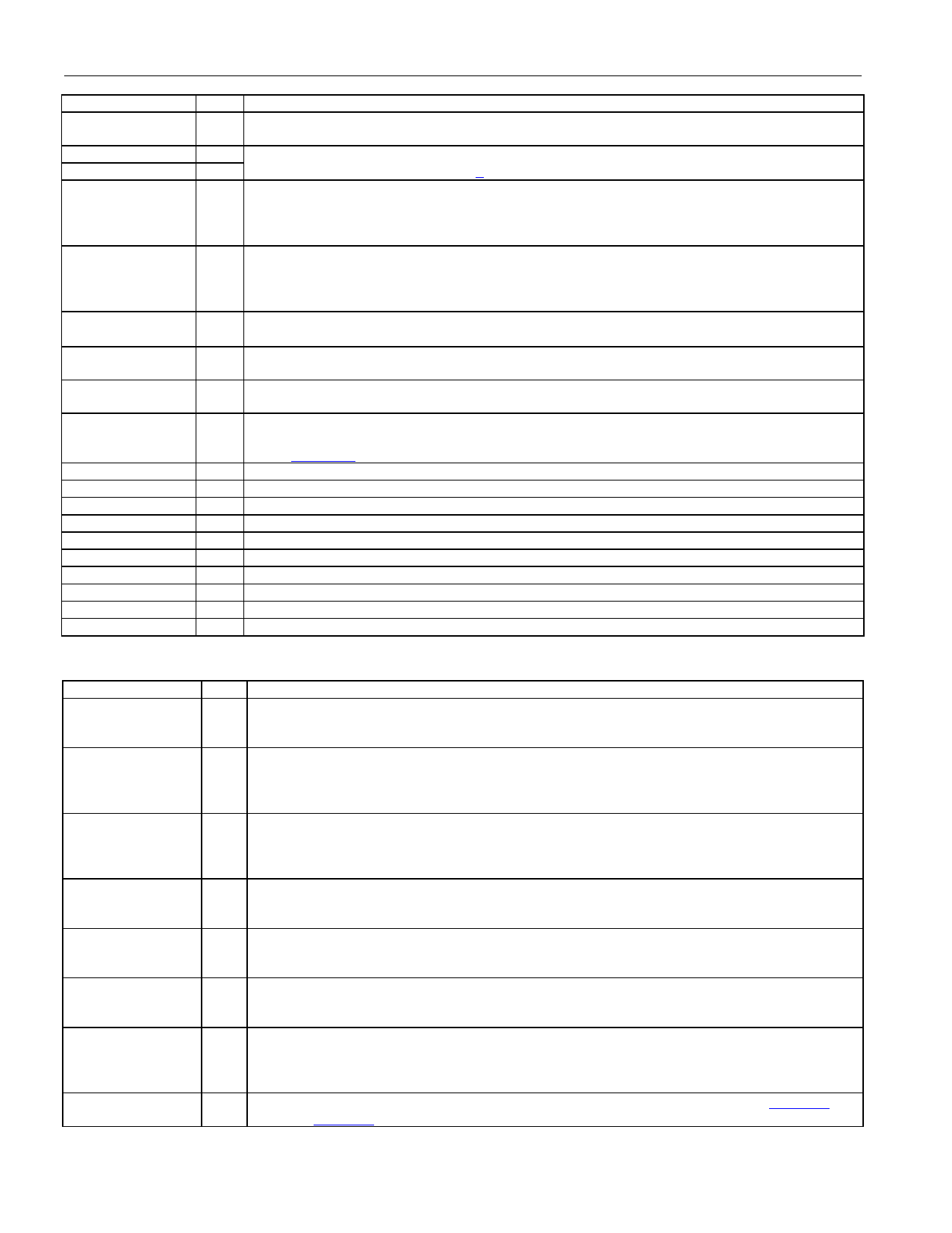
Table 2-E. Hardware Interface Mode Pin Description
PIN
ETS
NRZE
SCLKE
DJA
JAMUX
JAS
HBE
L0/L1/L2
I/O
FUNCTION
E1/T1 Select
I 0 = E1
1 = T1
NRZ Enable
I
0 = bipolar data at RPOS/RNEG and TPOS/TNEG
1 = NRZ data at RPOS and TPOS or TNEG; RNEG outputs a positive-going pulse when the
device receives a BPV, CV, or EXZ.
Receive and Transmit Synchronization Clock Enable. SCLKE combines RSCLKE (CCR5.3) and
I
TSCLKE (CCR5.2).
0 = disable 2.048MHz synchronization transmit and receive mode
1 = enable 2.048MHz synchronization transmit and receive mode
Disable Jitter Attenuator
I 0 = jitter attenuator enabled
1 = jitter attenuator disabled
Jitter Attenuator Clock Mux. Controls the source for JACLK.
I 0 = JACLK sourced from MCLK (2.048MHz or 1.544MHz at MCLK).
1 = JACLK sourced from internal PLL (2.048 MHz at MCLK).
Jitter Attenuator Path Select
I 0 = place the jitter attenuator on the receive side
1 = place the jitter attenuator on the transmit side
Receive and Transmit HDB3/B8ZS Enable. HBE combines RHBE (CCR2.3) and THBE
I
(CCR2.2).
0 = enable HDB3 (E1)/B8ZS (T1)
1 = disable HDB3 (E1)/B8ZS (T1)
I
Line Build-Out Select Bits 0,1, and 2. These pins set the transmitter build-out; see (Table 7-A
(E1) and Table 7-B (T1).
11 of 60
Share Link: 