ZR36067 データシートの表示(PDF) - Unspecified
部品番号
コンポーネント説明
一致するリスト
ZR36067 Datasheet PDF : 48 Pages
| |||
AV PCI CONTROLLER
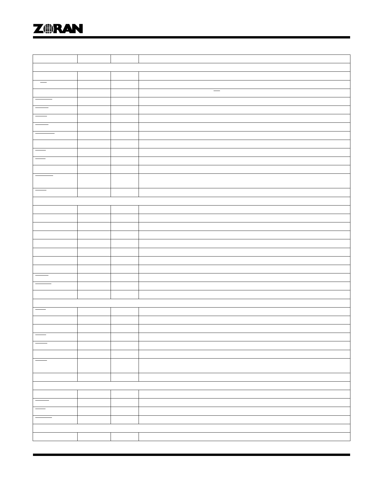
3.0 PIN DESCRIPTIONS
Symbol
Type [1]
Direction
Description
PCI Interface (48 pins)
AD[31:0]
3-state
I/O
Multiplexed address and data bus pins.
C/BE[3:0]
3-state
I/O
Bus commands or byte enables.
PAR
3-state
I/O
Even parity bit for AD31..0 and C/BE[3:0].
FRAME
3-state*
I/O
PCI cycle frame.
TRDY
3-state*
I/O
PCI target ready indicator.
IRDY
3-state*
I/O
PCI initiator ready.
STOP
3-state*
I/O
Indicates a target request to stop the current data transfer.
DEVSEL
3-state*
I/O
PCI device select, indicates that the target has decoded its address.
IDSEL
I
I
PCI initialization device select. Used as a chip-select to the ZR36067’s configuration space.
REQ
3-state
O
PCI bus request.
GNT
3-state
I
PCI bus grant.
PCICLK
I
I
PCI clock.
PCIRST
I
I
PCI reset. When active, all ZR36067 output pins are tri-stated. A low to high transition puts the
ZR36067 into its power-on reset state. Minimum active low duration is 3 PCI clocks.
INTA
open drain
O
PCI interrupt request A. A low level on this signal requests an interrupt from the host.
Digital Video Bus Interface (32 pins)
Y[7:0]/R[7:0]
3-state
I/O
Luminance/Red video lines. Also used to program the low byte of Subsystem Vendor ID.
UV[7:0]/G[7:0]
3-state
I/O
Chrominance/Green video lines. Also used to program the low byte of Subsystem ID.
B[7:0]
3-state
I/O
Blue video lines.
VCLKx2
I
I
Double frequency video bus clock.
VCLK
I
I
Digital video bus clock. Used as a qualifier to VCLKx2. Must be synchronized to VCLKx2.
HSYNC
3-state
I/O
Digital video bus horizontal sync.
VSYNC
3-state
I/O
Digital video bus vertical sync.
FI
I
I
Digital video bus field indicator (top/bottom).
PXEN
O
O
Active low Pixel Enable output to the ZR36016.
RTBSY
I
I
Active low Strip Memory Overflow/Underflow signal from the ZR36016.
START
O
O
Active high Start process output to the ZR36016.
GuestBus Interface (25 pins)
GCS[7:0]
O
O
Active low chip-select output to guest bus devices.
GADR[2:0]
O
O
Address outputs to guest bus devices.
GDAT[7:0]
3-state
I/O
Guest data bus. Also used to program the high byte of Subsystem Vendor ID.
GRD
O
O
Active low read output to guest bus devices.
GWR
O
O
Active low write output to guest bus devices.
GRDY
I
I
Active high “guest ready” input, used only in MPEG code-DMA mode as a data request.
GWS
I
I
Guest Wait-State indication. Assertion of this active-low input allows the guest device to extend
the GuestBus write (or read) cycle until it is capable of latching-in (or providing) the data.
GIRQ[1:0]
I
I
Positive-edge-sensitive interrupt request inputs from one or two of the guest bus slave devices.
CodecBus Interface (11 pins)
CODE[7:0]
3-state
I/O
Code Bus connected to the ZR36050.
CEND
I
I
Active low End of field process indication from the ZR36050.
CCS
I
I
Active low Code Bus active cycle signal from the ZR36050.
CBUSY
O
O
Active low Code FIFO Busy indication to the ZR36050.
I2C Bus Interface (2 pins)
SDA
OD
I/O
I2C bus data
7
Share Link: 