UPD72874 データシートの表示(PDF) - NEC => Renesas Technology
部品番号
コンポーネント説明
一致するリスト
UPD72874 Datasheet PDF : 40 Pages
| |||
µPD72874
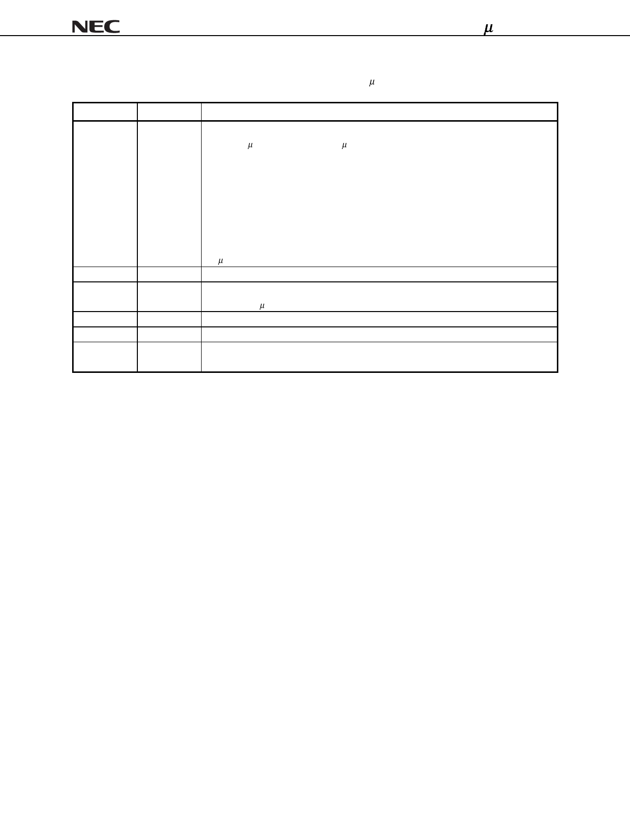
3.1.22 Offset_64 Power Management Control/Status Register
This is a 16-bit register that provides control status information of the µPD72874.
Bits
1,0
7-2
8
12-9
14,13
15
R/W
Description
R/W
PowerState Default value is undefined. This field is used both to determine the current power
state of the µPD72874 and to set the µPD72874 into a new power state.
00: D0 (DMA contexts: ON, Link Layer: ON, PME will be asserted upon INTA being active.)
01: D1 (DMA contexts: OFF, Link Layer: ON, PME will be asserted upon INTA being active)
10: D2 (DMA contexts: OFF, Link Layer: OFF, LPS: OFF, PME will be asserted upon
LinkON being active)
11: D3 (DMA contexts: OFF, Link Layer: OFF, LPS: OFF, PME will be asserted upon
LinkON being active)
The LPS is a PHY/Link interface signal and is defined in P1394a-2000. It is an internal signal in
the µPD72874.
R
Reserved Constant value of 000000.
R/W
PME_En Default value of 0. This field is used to enable the specific power management
features of the µPD72874.
R
Data_Select Constant value of 0000.
R
Data_Scale Constant value of 00.
R/W
PME_Status Default value is undefined. A write of ‘1’ clears this bit, while a write of ‘0’ is
ignored.
Preliminary Data Sheet S15306EJ2V0DS
25
Share Link: 