UPD72874 データシートの表示(PDF) - NEC => Renesas Technology
部品番号
コンポーネント説明
一致するリスト
UPD72874 Datasheet PDF : 40 Pages
| |||
µPD72874
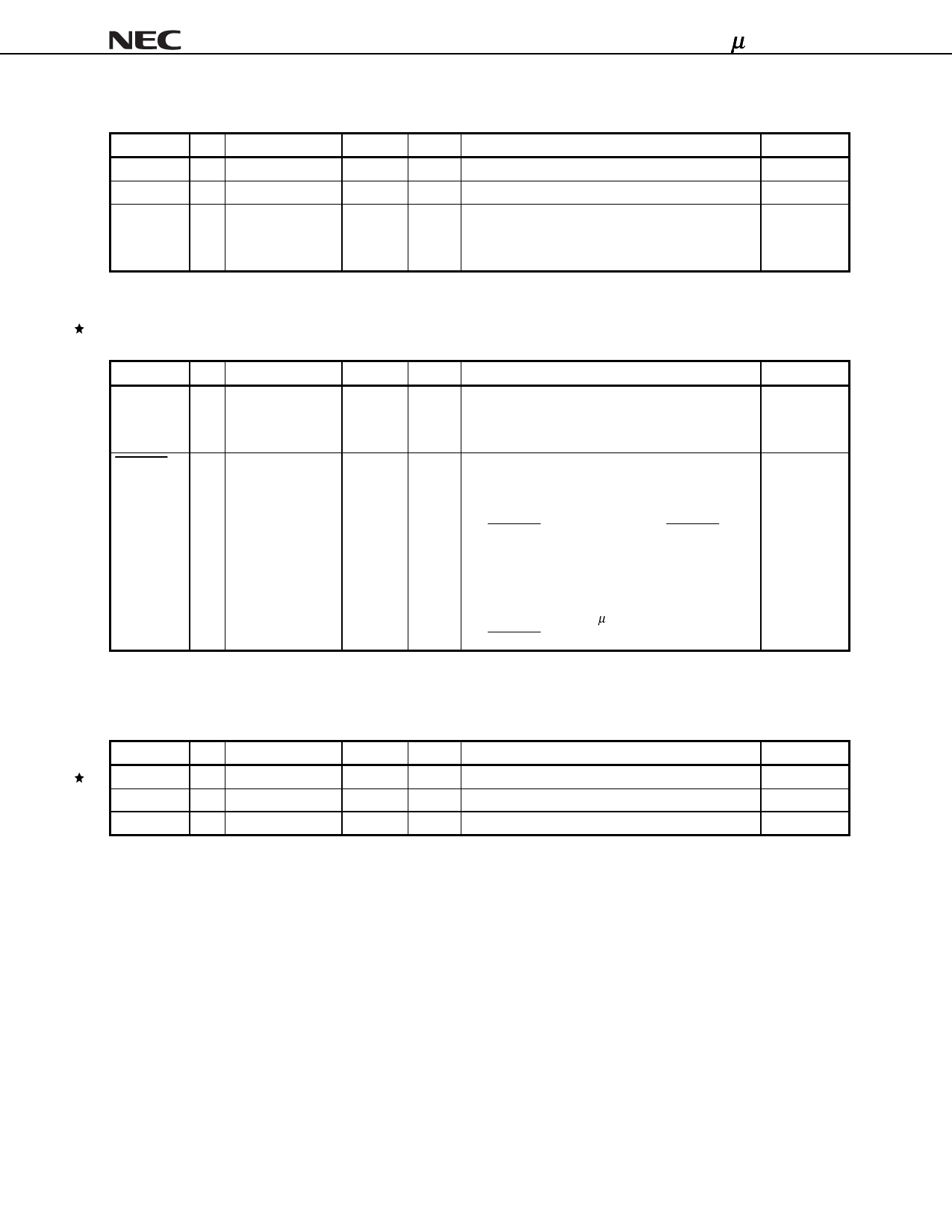
1.5 Serial ROM Interface Signals: (3 pins)
Name
I/O
Pin No.
IOL
Volts(V)
Function
GROM_SDA I/O 116
6 mA
3.3 Serial EEPROM Data Input / Output
GROM_SCL O 117
6 mA
3.3 Serial EEPROM Clock Output
GROM_EN I 118
-
3.3 Serial EEPROM Enable
1: GUID Load enable
0: GUID Load disable
Remark *: If the Link pin is pulled up, it should be connected to L_VDD.
1.6 D3cold Wake Up Function Signals: (2 pins)
Name
D3CSUP
I/O
Pin No.
I 114
RSMRST
I 74
IOL
Volts(V)
Function
-
5/3.3 D3cold Support
1: D3cold wake up enable
0: D3cold wake up disable
-
5/3.3 Resume Reset
D3cold support (114 pin) = ‘1’
As this mode supports D3cold wake up,
RSMRST must connect system RSMRST
signal.
D3cold support (114 pin) = ‘0’
As this mode is the µPD72872 compatible,
RSMRST clamp to ‘1’.
Remark *: If the Link pin is pulled up, it should be connected to L_VDD.
1.7 IC: (7 pins)
Name
I/O
Pin No.
IOL
Volts(V)
Function
IC(H)
I 75
-
- Internally Connected (High clamped)
IC(L)
I 76 to 78, 80, 115
-
- Internally Connected (Low clamped)
IC(N)
- 85
-
- Internally Connected (Open)
Remark *: If the Link pin is pulled up, it should be connected to L_VDD.
Block *
Link
Link
Link
Block *
Link
Link
Block *
Link
-
-
Preliminary Data Sheet S15306EJ2V0DS
11
Share Link: 