UPD72874 データシートの表示(PDF) - NEC => Renesas Technology
部品番号
コンポーネント説明
一致するリスト
UPD72874 Datasheet PDF : 40 Pages
| |||
µPD72874
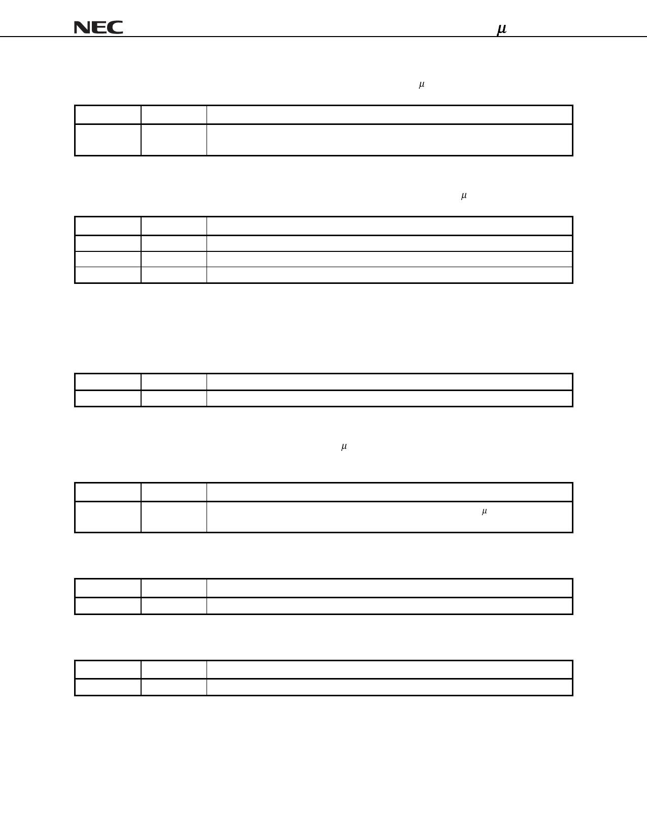
3.1.5 Offset_08 Revision ID Register
This register specifies a revision number assigned by NEC Corporation for the µPD72874.
Bits
7-0
R/W
Description
R
Default value of 01H. It specifies the silicon revision. It will be incremented for subsequent
silicon revisions.
3.1.6 Offset_09 Class Code Register
This register identifies the class code, sub-class code, and programming interface of the µPD72874.
Bits
7-0
15-8
23-16
R/W
Description
R
Constant value of 10H. It specifies an IEEE1394 OHCI-compliant Host Controller.
R
Constant value of 00H. It specifies an “IEEE1394” type.
R
Constant value of 0CH. It specifies a “Serial Bus Controller”.
3.1.7 Offset_0C Cache Line Size Register
This register specifies the system cache line size, which is PC-host system dependent, in units of 32-bit words.
The following cache line sizes are supported: 2, 4, 8, 16, 32, 64, and 128. All other values will be recognized as 0,
i.e. cache disabled.
Bits
7-0
R/W
R/W
Default value of 00H.
Description
3.1.8 Offset_0D Latency Timer Register
This register defines the maximum amount of time that the µPD72874 is permitted to retain ownership of the bus
after it has acquired bus ownership and initiated a subsequent transaction.
Bits
7-0
R/W
Description
R/W
Default value of 00H. It specifies the number of PCI-bus clocks that the µPD72874 may hold
the PCI bus as a bus-master.
3.1.9 Offset_0E Header Type Register
Bits
7-0
R/W
Description
R
Constant value of 00H. It specifies a single function device.
3.1.10 Offset_0F BIST Register
Bits
7-0
R/W
Description
R
Constant value of 00H. It specifies whether the device is capable of Built-in Self Test.
Preliminary Data Sheet S15306EJ2V0DS
21
Share Link: 