UPD72874 データシートの表示(PDF) - NEC => Renesas Technology
部品番号
コンポーネント説明
一致するリスト
UPD72874 Datasheet PDF : 40 Pages
| |||
µPD72874
2. PHY REGISTERS
2.1 Complete Structure for PHY Registers
0000
0001
0010
0011
0100
0101
0110
0111
1000
1001
1010
1011
1100
1101
1110
1111
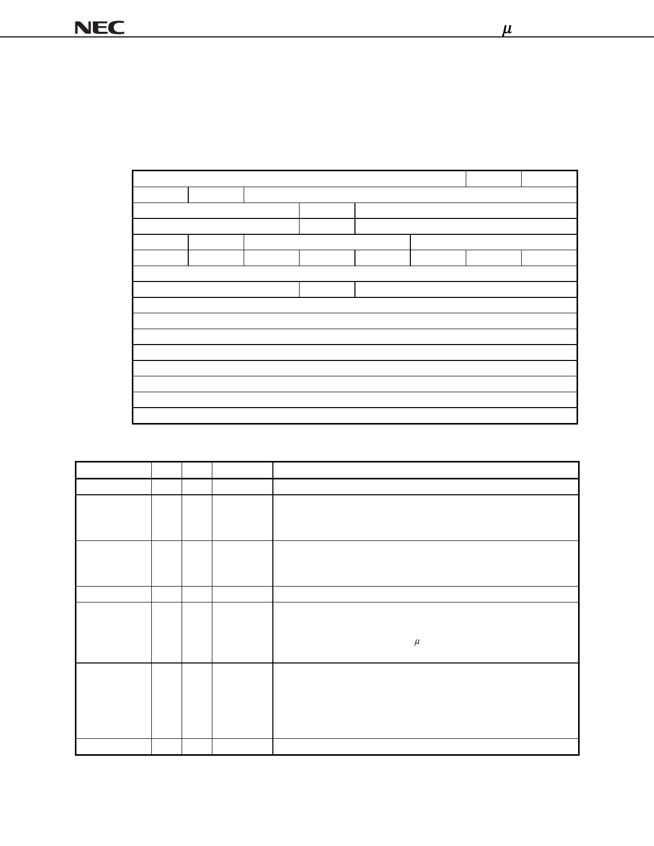
Figure 2-1. Complete Structure of PHY Registers
0
1
RHB
IBR
Extended (7)
Max_speed
Link_active Contender
Watchdog
ISBR
Page_select
2
3
4
5
6
7
Physical_ID
R
PS
Gap_count
Reserved
Total_ports
Reserved
Delay
Jitter
Pwr_class
Loop
Pwr_fail
Timeout Port_event Enab_accel Enab_multi
Reserved
Reserved
Port_select
Register0 (page_select)
Register1 (page_select)
Register2 (page_select)
Register3 (page_select)
Register4 (page_select)
Register5 (page_select)
Register6 (page_select)
Register7 (page_select)
Field
Physical_ID
R
PS
RHB
IBR
Gap_count
Extended
Table 2-1. Bit Field Description (1/3)
Size R/W Reset value
Description
6
R
000000 Physical_ID value selected from Self_ID period.
1
R
0
If this bit is 1, the node is root.
1: Root
0: Not root
1
R
Cable power status.
1: Cable power on
0: Cable power off
1 R/W
0
Root Hold -off bit. If 1, becomes root at the bus reset.
1 R/W
0
Initiate bus reset.
Setting to 1 begins a long bus reset.
Long bus reset signal duration: 166 µsec.
Returns to 0 at the beginning of bus reset.
6 R/W
111111 Gap count value.
It is updated by the changes of transmitting and receiving the PHY
configuration packet Tx/Rx.
The value is maintained after first bus reset.
After the second bus reset it returns to reset value.
3
R
111
Shows the extended register map.
Preliminary Data Sheet S15306EJ2V0DS
13
Share Link: 