PDI1394L21 データシートの表示(PDF) - Philips Electronics
部品番号
コンポーネント説明
一致するリスト
PDI1394L21 Datasheet PDF : 52 Pages
| |||
Philips Semiconductors
1394 full duplex AV link layer controller
Preliminary specification
PDI1394L21
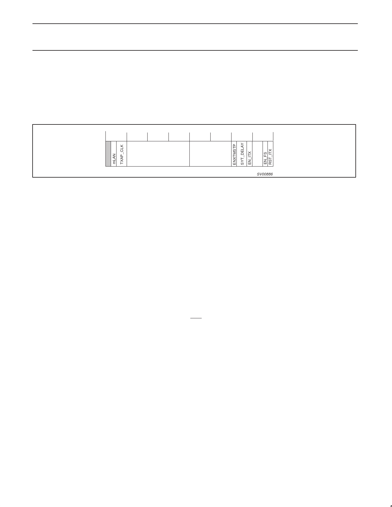
13.2 AV (Isochronous) Transmitter and Receiver Registers
13.2.1 Isochronous Transmit Packing Control and Status (ITXPKCTL) – Base Address: 0x020
This register allows the user to set up the appropriate AV packets from data entered into the AV interface. The packing and control parameters
(TRDEL, MAXBL, DBS, FN, QPC, and SPH) should never be changed while the transmitter is operating. The only exception to this is the
MAXBL parameter when in MPEG-2 packing mode.
NOTE: When reset of isochronous transmitter is necessary, first disable the transmitter (place bit 4, EN_ITX, LOW), wait for FIFO to empty, then
reset the transmitter (place RST_ITX, bit 0, HIGH). This procedure will ensure that data in the FIFO is transmitted before reset.
31 30 29 28 27 26 25 24 23 22 21 20 19 18 17 16 15 14 13 12 11 10 9 8 7 6 5 4 3 2 1 0
TRDEL
MAXBL
PM
SV00886
Reset Value 0x00000001
Bit 29..28:
R/W TXAP_CLK: Application Clock, default mode, ‘00’ the AVxCLK pin is an input. This pin can become an application
clock for the isochronous Transmitter (and output) by programming it to ‘01’, ‘10’, or ‘11’.
The programming values are:
00 Input
01 24.576MHz
10 12.288MHz
11 6.144MHz
Note that when enabled as ‘01’, ‘10’, or ‘11’, the AV port that is configured as transmitter and enabled will output this
clock signal on its AVxCLK pin.
Bit 27..16:
R/W TRDEL: Transport delay. Value added to cycle timer to produce time stamps. Lower 4 bits add to upper 4 bits of
cycle_offset, (Cycle Timer Register, CYCTM). Remainder adds to cycle_count field.
Bit 15..8:
R/W MAXBL: The (maximum) number of data blocks to be put in a payload.
Bit 7:
R/W ENXTMSTP: Enable External time stamp control. Allows an external time stamp (generated by the application) to be
inserted in place of the link-generated time stamp. Defaults to link generated time stamp. The application must
present the first byte of a quadlet-wide time stamp accompanied by the AVSYNC pulse (and AVVALID) to the
AVPORT. The external time stamp quadlet is inputted first, followed by the application data packet. The transmitted
packet size is now one quadlet larger than the original isochronous data packet—Set up the isochronous
transmitter accordingly with SPH = 1. CAUTION: Unless valid IEC 61883 time stamp format (based on the link cycle
timer) is used, the receiving node link chip must be equipped with a time stamp check disabling function similar to
the DIS_TSC bit (register 0X040, Bit 7). Please see section 13.2.8 for details.
Bit 6..5:
R/W SYT_DELAY: Programmable delay of AV1FSYNC and AV2FSYNC. Each cycle is 1 bus cycle, 125 ms.
Reset value is “00”, a 3 cycle delay.
01 = 2 cycles
00 = 3 cycles
10 = 4 cycles
11 = Reserved
Bit 4:
R/W EN_ITX: Enable receipt of new application packets and generation of isochronous bus packets in every cycle. This
bit also enables the Link Layer to arbitrate for the transmitter in each subsequent bus cycle. When this bit is disabled
(0), the current packet will be transmitted and then the transmitter will shut down.
Bit 3..2:
R/W PM: packing mode:
00 = variable sized bus packets, most generic mode.
01 = fixed size bus packets.
10 = MPEG–2 packing mode.
11 = No data, just CIP headers are transmitted.
Bit 1:
R/W EN_FS:enable generation/insertion of SYT stamps (Time Stamps) in CIP header.
Bit 0:
R/W Reset Isochronous Transmitter (RST_ITX): causes transmitter to be reset when ‘1’. In order for synchronous reset of
ITX to work properly, an AVxCLK (from either the internal or external source) must be present and ensure that the
reset bit is kept (programmed) HIGH for at least the duration of one AVxCLK period. Failure to do so may cause
the application interface of this module to be improperly reset (or not reset at all). When reset is enabled, all bytes
will be flushed from the FIFO and transmission will cease immediately.
1999 Aug 06
33
Share Link: 