PDI1394L21 データシートの表示(PDF) - Philips Electronics
部品番号
コンポーネント説明
一致するリスト
PDI1394L21 Datasheet PDF : 52 Pages
| |||
Philips Semiconductors
1394 full duplex AV link layer controller
Preliminary specification
PDI1394L21
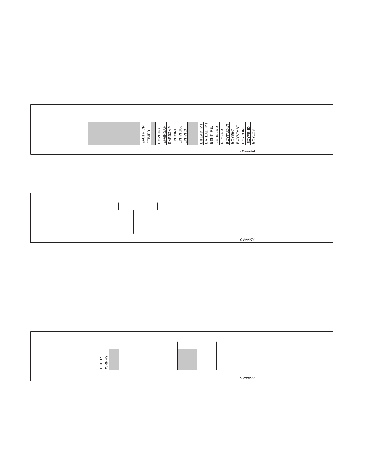
13.1.4 Link / Phy Interrupt Enable (LNKPHYINTE) – Base Address: 0x00C
This register is a mirror of the Link/Phy Interrupt Acknowledge (LNKPHYINTACK) register. Enabling an interrupt is accomplished by writing a ‘1’
to the bit corresponding to the interrupt desired.
This register enables the interrupts described in the Link /Phy Interrupt Acknowledge register (LNKPHYINTACK) description. A one in any of the
bits enables that function to create an interrupt. A zero disables the interrupt, however the status is readable in the Link /Phy Interrupt
Acknowledge register.
31 30 29 28 27 26 25 24 23 22 21 20 19 18 17 16 15 14 13 12 11 10 9 8 7 6 5 4 3 2 1 0
Reset Value 0x00000000
Bits 18..0 are interrupt enable bits for the Link/Phy Interrupt Acknowledge (LNKPHYINTACK).
SV00894
13.1.5 Cycle Timer Register (CYCTM) – Base Address: 0x010
Cycle Timer Register operation is controlled by the Cycle Timer Enable (CYTMREN) bit in the Link Control Register (LNKCTL, 0x004).
3130 29 28 27 26 25 24 23 22 21 20 19 18 17 16 15 14 13 12 11 10 9 8 7 6 5 4 3 2 1 0
CYCLE_SECONDS
CYCLE_NUMBER
CYCLE_OFFSET
Reset Value 0x00000000
Bit 31..25:
R/W Seconds count: 1-Hz cycle timer counter.
Bit 24..12:
R/W Cycle Number: 8kHz cycle timer counter.
Bit 11..0:
R/W Cycle Offset: 24.576MHz cycle timer counter.
SV00276
13.1.6 Phy Register Access (PHYACS) – Base Address: 0x014
This register provides access to the internal registers on the Phy. There are special considerations when reading or writing to this register. When
reading a PHY register, the address of the register is written to the PHYRGAD field with the RDPHY bit set. The PHY data will be valid when the
PHYRRX bit (LNKPHYINTACK register bit 14) is set. Once this happens the register data is available in the PHYRXDATA, the address of the
register just read is also available in the PHYRXAD fields. When writing a Phy register, the address of the register to be written is set in the
PHYRGAD field and the data to be written to the register is set in PHYRGDATA, along with the WRPHY bit being set. Once the write is
complete, the WRPHY bit will be cleared. Do not write a new Read/Write command until the previous one has been completed. After the Self-ID
phase, PHY register 0 will be read automatically.
31 30 29 28 27 26 25 24 23 22 21 20 19 18 17 16 15 14 13 12 11 10 9 8 7 6 5 4 3 2 1 0
PHYRGAD
PHYRGDATA
PHYRXAD
PHYRXDATA
SV00277
Reset Value 0x00000000
Bit 31:
R/W Read Phy Chip Register (RDPHY): When asserted, the PDI1394L21 sends a read register request with address
equal to Phy Rg Ad to the Phy interface. This bit is cleared when the request is sent.
Bit 30:
R/W Write Phy Chip Register (WRPHY): When asserted, the PDI1394L21 sends a write register request with address
equal to Phy Rg Ad to the Phy interface. This bit is cleared when the request is sent.
Bit 27..24:
R/W Phy Chip Register Address (PHYRGAD): This is the address of the Phy-chip register that is to be accessed.
Bit 23..16:
R/W
Phy Chip Register Data (PHYRGDATA): This is the data to be written to the Phy-chip register indicated in Phy Rg Ad.
Bit 11..8:
R
Phy Chip Register Received Address (PHYRXAD): Address of register from which Phy Rx Data came.
Bit 7..0:
R
Phy Chip Register Received Data (PHYRXDATA): Data from register addressed by Phy Rx Ad.
1999 Aug 06
31
Share Link: 