07XSC200 データシートの表示(PDF) - Freescale Semiconductor
部品番号
コンポーネント説明
一致するリスト
07XSC200 Datasheet PDF : 51 Pages
| |||
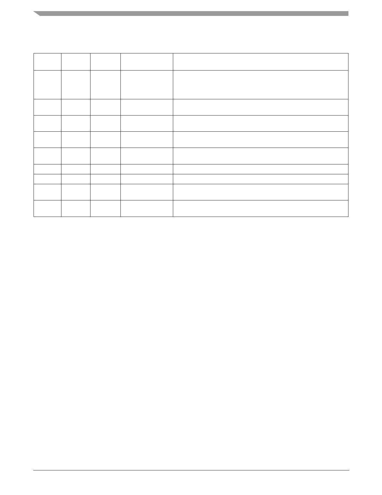
Table 1. 07XSC200 Pin Definitions (continued)
Pin
Number
Pin Name
Pin
Function
Formal Name
Definition
8, 33
VPWR
Power
Positive Power Supply Pin 8 is a positive supply for quiet and accurate control. Pin 33 is a power supply
for the high current switch. These pins must be shorted at board level.
Connecting a heatsink to pin 33 guarantees optimal heat-evacuation
properties.
9 to 16
HS1
Output
High Side Output Protected 7.0 m high side power output pin to the load. Those pins must be
shorted at board level.
26
FSI
Input
Fail-safe Input
The value of the resistance connected between this pin and ground determines
the state of the outputs after a watchdog time-out occurs.
27
CSNS
Output
Output Current This pin is used to output a current proportional to the designated HS0-1 output.
Monitoring
28
CLOCK
Input
Reference Clock This pin is used to apply a reference clock used to control the outputs in PWM
mode through embedded PWM module.
29
IN0
Input
Direct Input 0
This input pin is used to directly control the output HS0.
30
IN1
Input
Direct Input 1
This input pin is used to directly control the output HS1.
31
FSB
Output
Fault Status (Active This is an open drain configured output requiring an external pull-up resistor to
Low)
VDD for fault reporting.
32
WAKE
Input
Wake
This pin is used to input a Logic [1] signal so as to enable the watchdog timer
function.
07XSC200
4
Analog Integrated Circuit Device Data
Freescale Semiconductor
Share Link: 