SCN2651CC1N28 データシートの表示(PDF) - Philips Electronics
部品番号
コンポーネント説明
一致するリスト
SCN2651CC1N28 Datasheet PDF : 15 Pages
| |||
Philips Semiconductors
Programmable communications interface (PCI)
Product specification
SCN2651
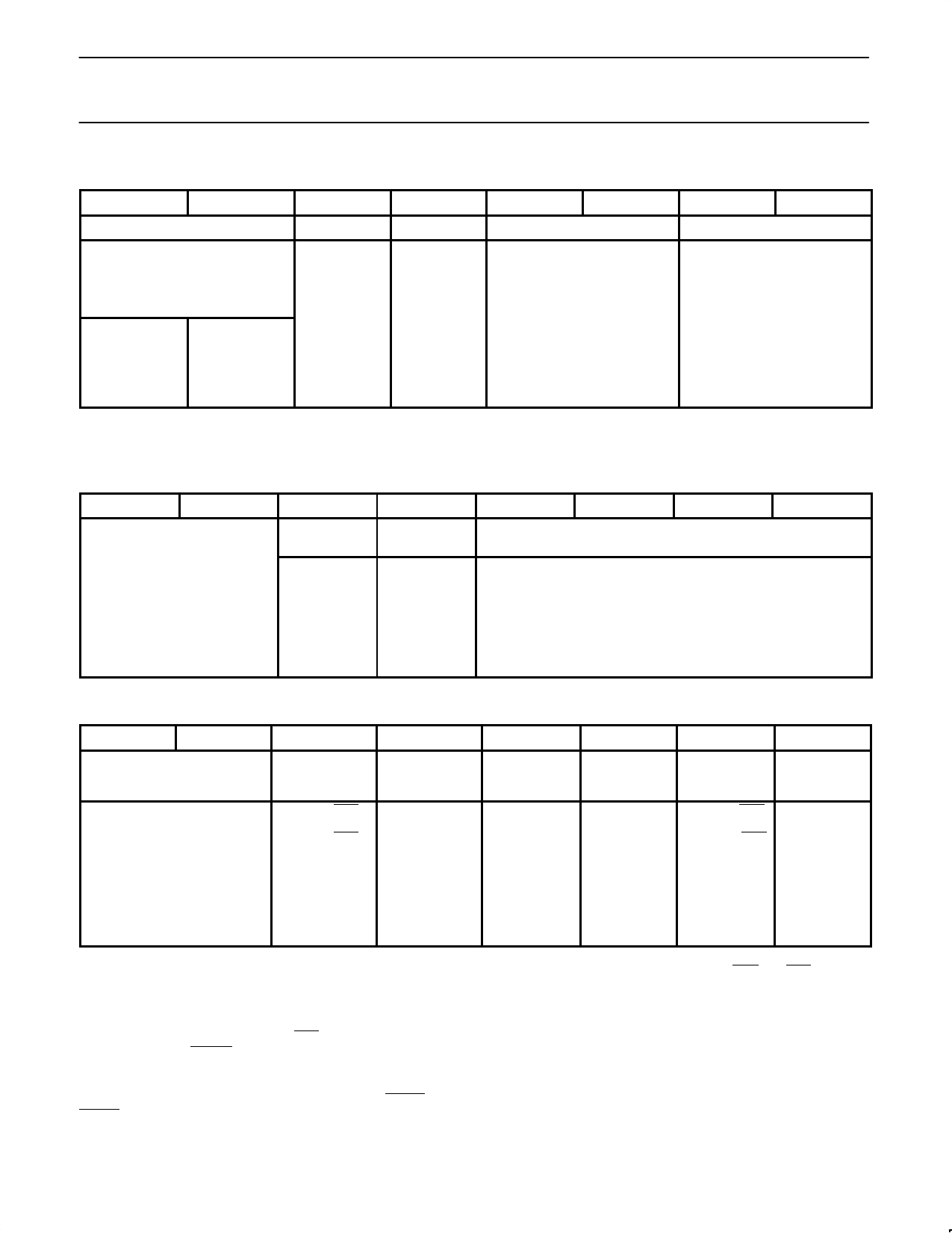
Table 5. Mode Register 1 (MR1)
MR17
MR16
MR15
MR14
MR13
MR12
MR11
MR10
Async: Stop bit length
00 = Invalid
01 = 1 Stop bit
10 = 1 1/2 Stop bits
11 = 2 Stop bits
Sync:
Sync:
Number of SYN Transparency
char
control
Parity Type
0 = Odd
1 = Even
Parity Control
0 = Disabled
1 = Enabled
Character Length
00 = 5 Bits
01 = 6 Bits
10 = 7 Bits
11 = 8 Bits
Mode and Baud Rate Factor
00 = Synchronous 1X rate
01 = Asynchronous 1X rate
10 = Asynchronous 16X rate
11 = Asynchronous 64X rate
0 = Double SYN 0 = Normal
1 = Single SYN 1 = Transparent
NOTE:
Baud rate factor in asynchronous applies only if external clock is selected. Factor is 16X if internal clock is selected. Mode must be selected
(MR11, MR10) in any case.
Table 6. Mode Register 2 (MR2)
MR27
MR26
MR25
Transmitter
Clock
Not used
0 = External
1 = Internal
MR24
Receiver
Clock
0= External
1 = Internal
MR23
MR22
MR21
Baud Rate Selection
MR20
0000 = 50 Baud
0001 = 75
0010 = 110
0011 = 134.5
0100 = 150
0101 = 300
0110 = 600
0111 = 1200
1000 = 1800 Baud
1001 = 2000
1010 = 2400
1011 = 3600
1100 = 4800
1101 = 7200
1110 = 9600
1111 = 19,200
Table 7. Command Register (CR)
CR7
CR6
CR5
Operating Mode
Request
to Send
00 = Normal operation
01 = Async: automatic
echo mode
Sync: SYN and/or DLE
stripping mode
10 = Local Loopback
11 = Remote Loopback
0 = Force RTS
output high
1 = Force RTS
output low
CR4
CR3
Reset Error
0 = Normal
1 = Reset
error flag
in status reg
(FE, OE,
PE/DLE
DETECT)
Async:
Force Break
0 = Normal
1 = Force
break
Sync
Send DLE
0 = Normal
1 = Send DLE
CR2
Receive
Control
(RxEN)
0 = Disable
1 = Enable
CR1
CR0
Data Terminal
Ready
Transmit
Control
(TxEN)
0 = Force DTR
output high
1 = Force DTR
output low
0 = Disable
1 = Enable
Command Register (CR)
Table 7 illustrates the command register. Bits CR0 (TxEN) and CR2
(RxEN) enable or disable the transmitter and receiver respectively.
A 0 to 1 transition of CR2 forces start bit search (async mode) or
hunt mode (sync mode) on the second RxC rising edge. Disabling
the receiver causes RxRDY to go high (inactive). If the transmitter
is disabled, it will complete the transmission of the character in the
transmit shift register (if any) prior to terminating operation. The TxD
output will then remain in the marking state (high) while TxRDY and
TxEMT will go high (inactive). If the receiver is disabled, it will
terminate operation immediately. Any character being assembled
will be neglected.
Bits CR1 (DTR) and CR5 (RTS) control the DTR and RTS outputs.
Data at the outputs is the logical complement of the register data.
In asynchronous mode, setting CR3 will force and hold the TxD
output low (spacing condition) at the end of the current transmitted
character. Normal operation resumes when CR3 is cleared. The
TxD line will go high for at least one bit time before beginning
transmission of the next character in the transmit data holding
register. In synchronous mode, setting CR3 causes the
transmission of the DLE register contents prior to sending the
character in the transmit data holding register. CR3 should be reset
in response to the next TxRDY.
1994 Apr 27
8
Share Link: 