SCN2651CC1N28 データシートの表示(PDF) - Philips Electronics
部品番号
コンポーネント説明
一致するリスト
SCN2651CC1N28 Datasheet PDF : 15 Pages
| |||
Philips Semiconductors
Programmable communications interface (PCI)
Product specification
SCN2651
required number of accesses are made, the internal sequencer
recycles to point at the first register. The pointers are reset to SYN1
register and mode register 1 by a RESET input or by performing a
“read command register” operation, but are unaffected by any other
read or write operation.
The SCN2651 register formats are summarized in Tables 5, 6, 7 and
8. Mode registers 1 and 2 define the general operational
characteristics of the PCI, while the command register controls the
operation within this basic framework. The PCI indicates its status
in the status register. These registers are cleared when a RESET
input is applied.
Mode Register 1 (MR1)
Table 5 illustrates mode register 1. Bits MR11 and MR10 select the
communication format and baud rate multiplier. 00 specifies
synchronous mode and 1X multiplier. 1X, 16X, and 64X multipliers
are programmable for asynchronous format. However, the multiplier
in asynchronous format applies only if the external clock input option
is selected by MR24 or MR25.
MR13 and MR12 select a character length of 5, 6, 7, or 8 bits. The
character length does not include the parity bit, if programmed, and
does not include the start and stop bits in asynchronous mode.
MR14 controls parity generation. If enabled, a parity bit is added to
the transmitted character and the receiver performs a parity check
on incoming data. MR15 selects odd or even parity when parity is
enabled by MR14.
In asynchronous mode, MR17 and MR16 select character framing of
1, 1.5, or 2 stop bits. (If 1X baud rate is programmed, 1.5 stop bits
default to 1 stop bit on transmit.) In synchronous mode, MR17
controls the number of SYN characters used to establish
synchronization and for character fill when the transmitter is idle.
SYN1 alone is used if MR17 = 1, and SYN1–SYN2 is used when
MR17 = 0. If the transparent mode is specified by MR16,
DLE–SYN1 is used for character fill and SYN detect, but he normal
synchronization sequence is used. Also DLE stripping and DLE
detect (with MR14 = 0) are enabled.
Mode Register 2 (MR2)
Table 6 illustrates mode register 2. MR23, MR22, MR21, and MR20
control the frequency of the internal baud rate generator (BRG).
Sixteen rates are selectable. When driven by a 5.0688MHz input at
the BRCLK input (Pin 20), the BRG output has zero error except at
134.5 2000, and 19,200 baud, which have errors of +0.016%,
+0.235%, and +3.125% respectively.
Table 4. SCN2651 Register Addressing
CE A1 A0 R/W
FUNCTION
1
X
X
X 3-State data bus
0
0
0
0 Read receive holding register
0
0
0
1 Write transmit holding register
0
0
1
0 Read status register
0
0
1
1 Write SYN1/SYN2/DLE registers
0
1
0
0 Read mode registers 1/2
0
1
0
1 Write mode registers 1/2
0
1
1
0 Read command register
0
1
1
1 Write command register
NOTE: See AC Characteristics section for timing requirements.
MR25 and MR24 select either the BRG or the external inputs TxC
and RxC as the clock source for the transmitter and receiver,
respectively. If the BRG clock is selected, the baud rate factor in
asynchronous mode is 16X regardless of the factor selected by
MR11 and MR10. In addition, the corresponding clock pin provides
an output at 1X the baud rate.
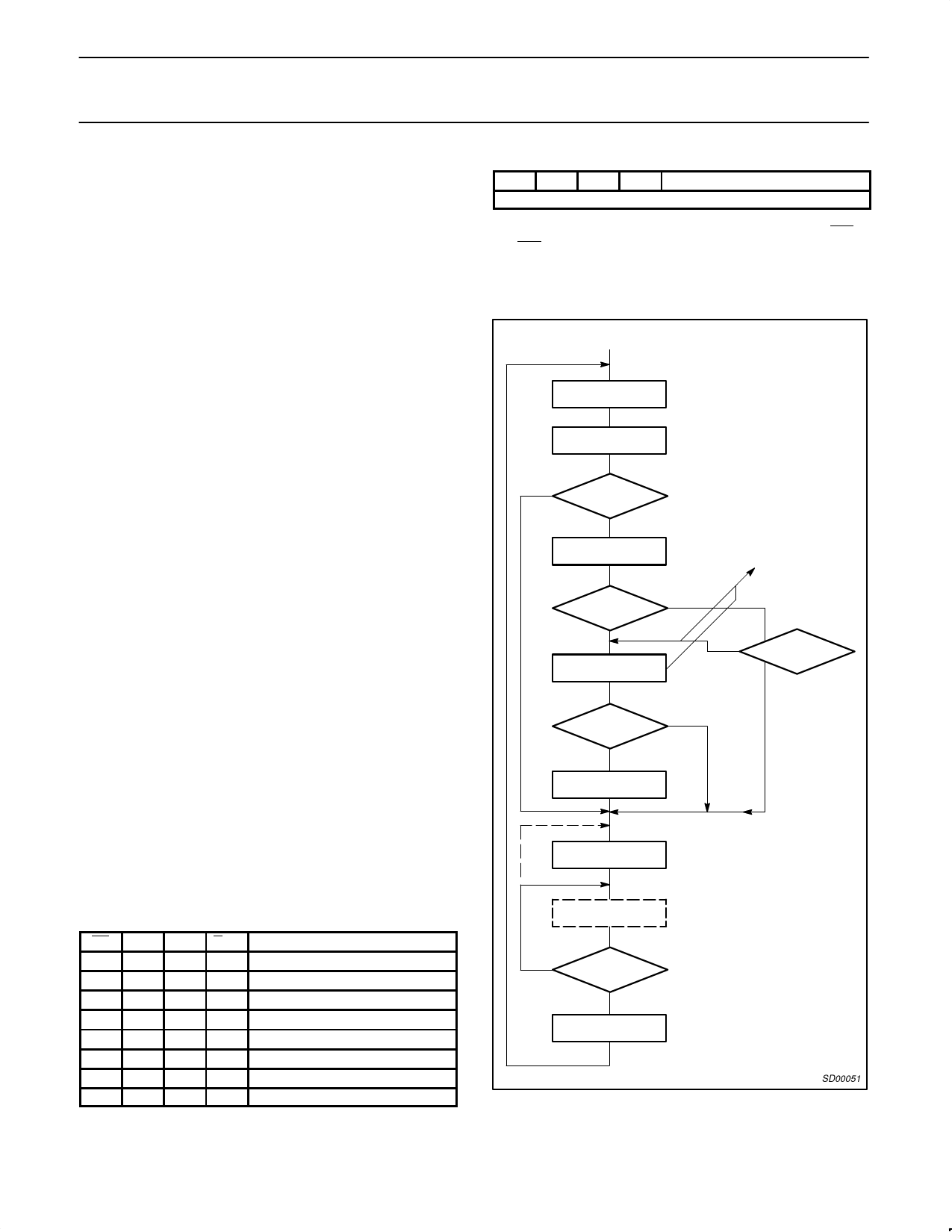
INITIAL RESET
LOAD
MODE REGISTER 1
LOAD
MODE REGISTER 2
NOTE:
Mode Register 1 must be written
before 2 can be written. Mode Register 2
need not be programmed if external
clocks are used.
N
SYNCHRONOUS?
Y
LOAD
SYN 1 REGISTER
NOTE:
SYN1 Register must be written
before SYN2 can be written, and
SYN2 before DLE can be written.
DOUBLE
N
SYNC?
Y
LOAD
SYN 2 REGISTER
TRANSPARENT
N
MODE?
Y
LOAD
DLE REGISTER
Y
TRANSPARENT
MODE?
N
LOAD
COMMAND REGISTER
OPERATE
N
RECONFIGURE?
Y
DISABLE
RCVR AND XMTR
SD00051
Figure 1. SCN2651 Initialization Flowchart
1994 Apr 27
7
Share Link: 