SCN2651CC1N28 データシートの表示(PDF) - Philips Electronics
部品番号
コンポーネント説明
一致するリスト
SCN2651CC1N28 Datasheet PDF : 15 Pages
| |||
Philips Semiconductors
Programmable communications interface (PCI)
Product specification
SCN2651
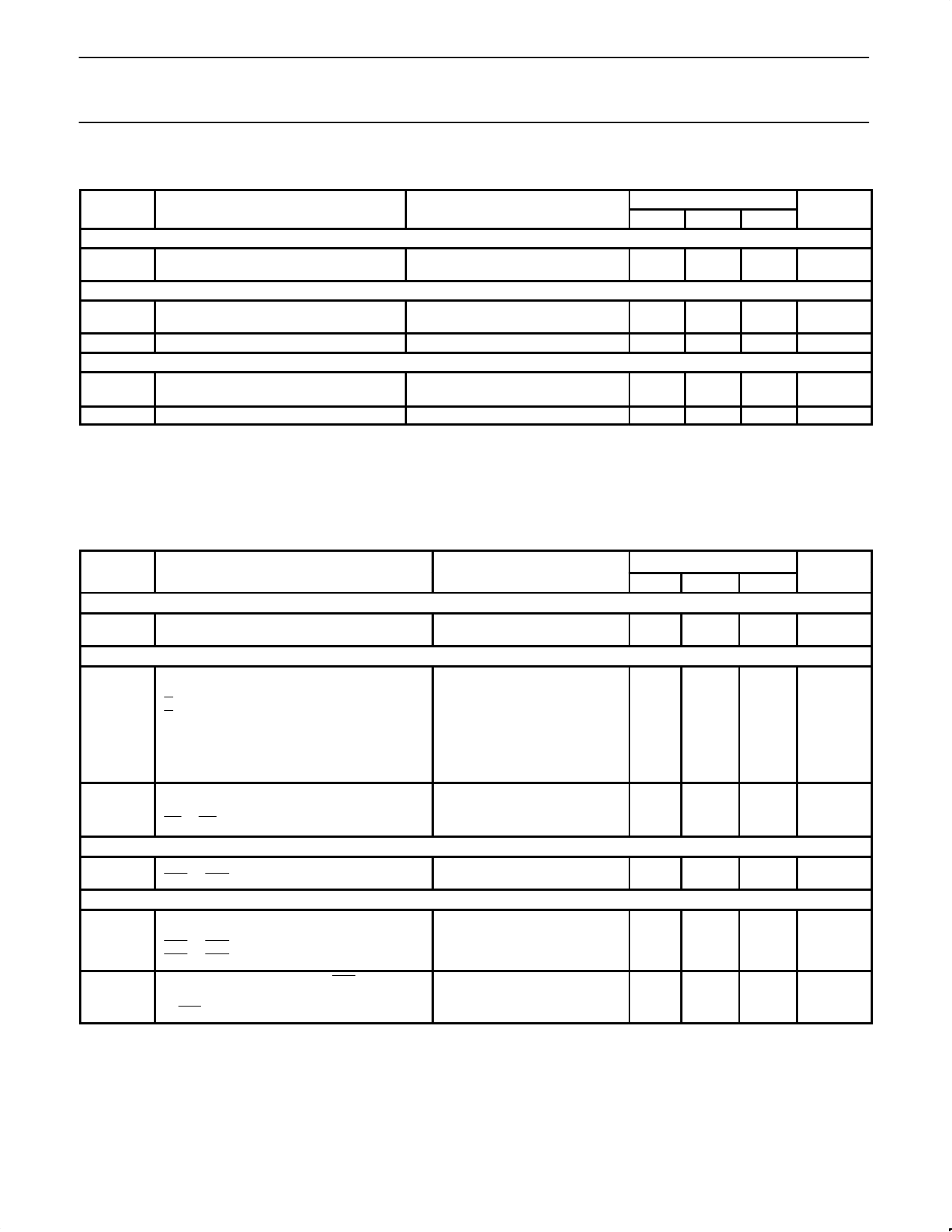
DC ELECTRICAL CHARACTERISTICS1, 2, 3
SYMBOL
PARAMETER
TEST CONDITIONS
LIMITS
Min
Typ
Max
UNIT
Input voltage
VIL
Low
VIH
High
Output voltage
2.0
0.8
V
V
VOL
VOH
Low
High
IIL
Input leakage current
3-State output leakage current
IOL = 1.6mA
IOH = -100µA
2.4
VIN = 0 to 5.25V
-10
0.4
V
V
10
µA
ILH
Data bus high
ILL
Data bus low
VO = 4.0V
VO = 0.45V
-10
10
µA
-10
10
µA
ICC
Power supply current
150
mA
NOTES:
1. Parameters are valid over operating temperature range unless otherwise specified. See ordering code table for applicable temperature
range and operating supply range.
2. All voltage measurements are referenced to ground. All time measurements are at the 50% level for inputs (except tBRH and tBRL) and at
0.8V and 2.0V for outputs. Input levels for testing are 0.45V and 2.4V.
3. Typical values are at +25°C, typical supply voltages and typical processing parameters.
AC ELECTRICAL CHARACTERISTICS1, 2, 3
LIMITS
SYMBOL
PARAMETER
TEST CONDITIONS
Min
Typ
Max
UNIT
Pulse width
tRES
tCE
Reset
Chip enable
Set-up and hold time
1000
ns
300
ns
tAS
tAH
tCS
tCH
tDS
tDH
tRXS
tRXH
Address setup
Address hold
R/W control setup
R/W control hold
Data setup for write
Data hold for write
RX data setup
RX data hold
20
ns
20
ns
20
ns
20
ns
225
ns
0
ns
300
ns
350
ns
tDD
tDF
tCED
Data delay time for read
Data bus floating time for read
CE to CE delay
CL = 100pF
CL = 100pF
700
250
ns
150
ns
ns
Input clock frequency
fBRG
fR/T6
Baud rate generator
TxC or RxC
Clock width
tBRH5
tBRL5
tR/TH
tR/TL6
Baud rate high
Baud rate low
TxC or RxC high
TxC or RxC low
tTXD
TxD delay from falling edge of TxC
tTCS
Skew between TxD changing and falling edge
of TxC output4
CL = 100pF
CL = 100pF
1.0 5.0688 5.0738
dc
1.0
70
70
500
500
650
0
MHz
MHz
ns
ns
ns
ns
ns
ns
NOTES:
1. Parameters are valid over operating temperature range unless otherwise specified. See ordering code table for applicable temperature
range and operating supply range.
2. All voltage measurements are referenced to ground. All time measurements are at the 50% level for inputs (except tBRH and tBRL) and at
0.8V and 2.0V for outputs. Input levels for testing are 0.45V and 2.4V.
3. Typical values are at +25°C, typical supply voltages and typical processing parameters.
4. Parameter applies when internal transmitter clock is used.
5. Under test conditions of 5.0688MHz, fBRG, tBRH, and tBRL measured at VIH and VIL respectively.
6. tR/T and tR/TL shown for all modes except local loopback. For local loopback mode fR/T = 0.7MHz and tR/TL = 700ns min.
1994 Apr 27
3
Share Link: 