NM34C02 データシートの表示(PDF) - Fairchild Semiconductor
部品番号
コンポーネント説明
一致するリスト
NM34C02 Datasheet PDF : 12 Pages
| |||
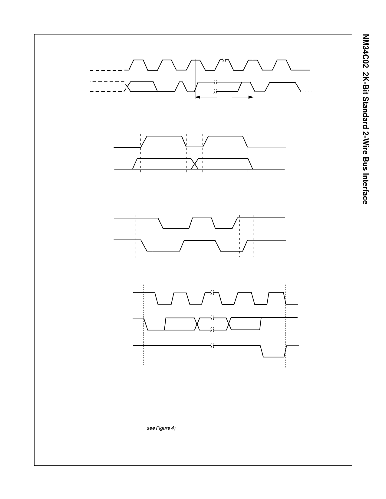
Write Cycle Timing
SCL
SDA
8th BIT
WORD n
ACK
STOP
CONDITION
tWR
START
CONDITION
DS012821-6
SCL
SDA
DATA STABLE
DATA
CHANGE
Data Validity (Figure 1).
SCL
SDA
START
CONDITION
STOP
CONDITION
DS012821-7
Start and Stop Definition (Figure 2).
DS012821-8
SCL FROM
MASTER
1
8
9
DATA OUTPUT
FROM
TRANSMITTER
DATA OUTPUT
FROM
RECEIVER
START
ACKNOWLEDGE
Acknowledge Responses from Receiver (Figure 3).
DS012821-9
Device Addressing
Following a start condition the master must output the address of
the slave it is accessing. The most significant four bits of the slave
address are those of the device type identifier (see Figure 4). This
is fixed as 1010 for all EEPROM devices.
All IIC EEPROMs use an internal protocol that defines a PAGE
BLOCK size of 2K bits (for Byte addresses 00 through FF).
NM34C02 Rev. D.2
7
www.fairchildsemi.com
Share Link: 