NM34C02 データシートの表示(PDF) - Fairchild Semiconductor
部品番号
コンポーネント説明
一致するリスト
NM34C02 Datasheet PDF : 12 Pages
| |||
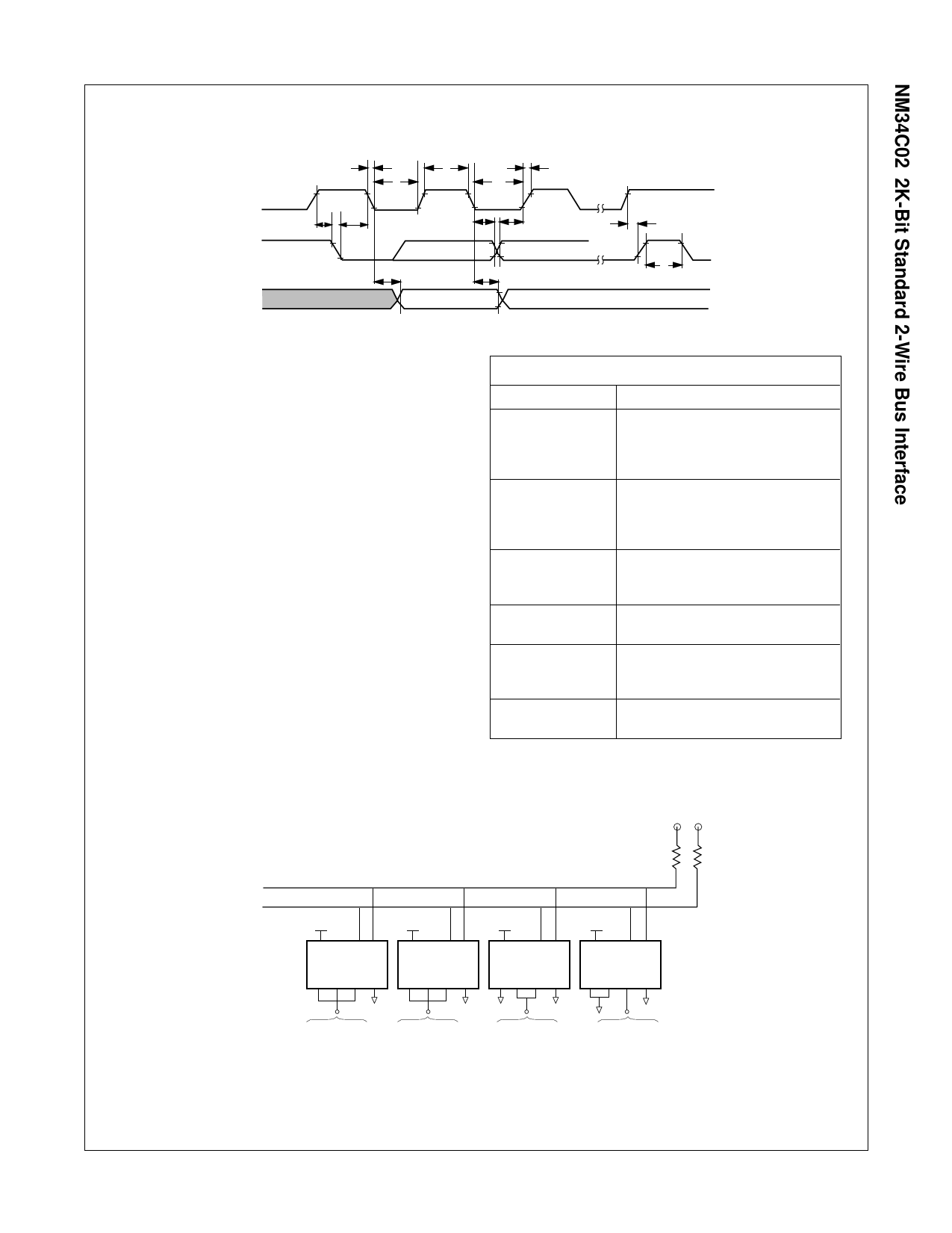
Bus Timing
tF
tHIGH
tLOW
SCL
SDA
tSU:STA
tHD:STA
tHD:DAT
,,IN
tAA
SDA
OUT
Background Information (IIC Bus)
As mentioned, the IIC bus allows synchronous bidirectional com-
munication between Transmitter/Receiver using the SCL (clock)
and SDA (Data I/O) lines. All communication must be started with
a valid START condition, concluded with a STOP condition and
acknowledged by the Receiver with an ACKNOWLEDGE condi-
tion.
In addition, since the IIC bus is designed to support other devices
such as RAM, EPROMs, etc., a device type identifier string must
follow the START condition. For EEPROMs, this 4-bit string is
1010. Also refer the Addressing the WP Register section.
As shown below, although the EEPROMs on the IIC bus may be
configured in any manner required, the total memory addressed can
not exceed 16K (16,384 bits) on the Standard IIC protocol. EE-
PROM memory address programming is controlled by 2 methods:
• Hardware configuring the A0, A1, and A2 pins (Device
Address pins) with pull-up or pull-down resistors. All unused
pins must be grounded (tied to VSS).
• Software addressing the required PAGE BLOCK within the
device memory array (as sent in the Slave Address string).
Addressing an EEPROM memory location involves sending a
command string with the following information:
[DEVICE TYPE]—[DEVICE ADDRESS]—[PAGE BLOCK
ADDRESS]—[BYTE ADDRESS]
tR
tLOW
tSU:DAT
tSU:STO
tDH
tBUF
DS012821-4
BYTE
PAGE
PAGE BLOCK
MASTER
SLAVE
TRANSMITTER
RECEIVER
DEFINITIONS
8 bits of data
16 sequential addresses (one byte
each) that may be programmed
during a 'Page Write' programming
cycle
2,048 (2K) bits organized into 16
pages of addressable memory. (8
bits) x (16 bytes) x (16 pages) = 2,048
bits
Any IIC device CONTROLLING the
transfer of data (such as a micropro-
cessor)
Device being controlled (EEPROMs
are always considered Slaves)
Device currently SENDING data on
the bus (may be either a Master or
Slave).
Device currently receiving data on the
bus (Master or Slave)
Example of 16K of Memory on 2-Wire Bus
VCC
SDA
SCL
VCC
VCC
VCC
VCC
NM34C02L
A0 A1 A2 VSS
NM24C02
A0 A1 A2 VSS
NM24C04
A0 A1 A2 VSS
NM24C08
A0 A1 A2 VSS
To VCC or VSS
To VCC or VSS
To VCC or VSS
Note:
The SDA pull-up resistor is required due to the open-drain/open collector output of IIC bus devices
The SCL pull-up resistor is recommended because of the normal SCL line inactive 'high' state.
It is recommended that the total line capacitance be less than 400pF.
Specific timing and addressing considerations are described in greater detail in the following sections.
To VCC or VSS
DS012821-5
NM34C02 Rev. D.2
5
www.fairchildsemi.com
Share Link: 