NM34C02 データシートの表示(PDF) - Fairchild Semiconductor
部品番号
コンポーネント説明
一致するリスト
NM34C02 Datasheet PDF : 12 Pages
| |||
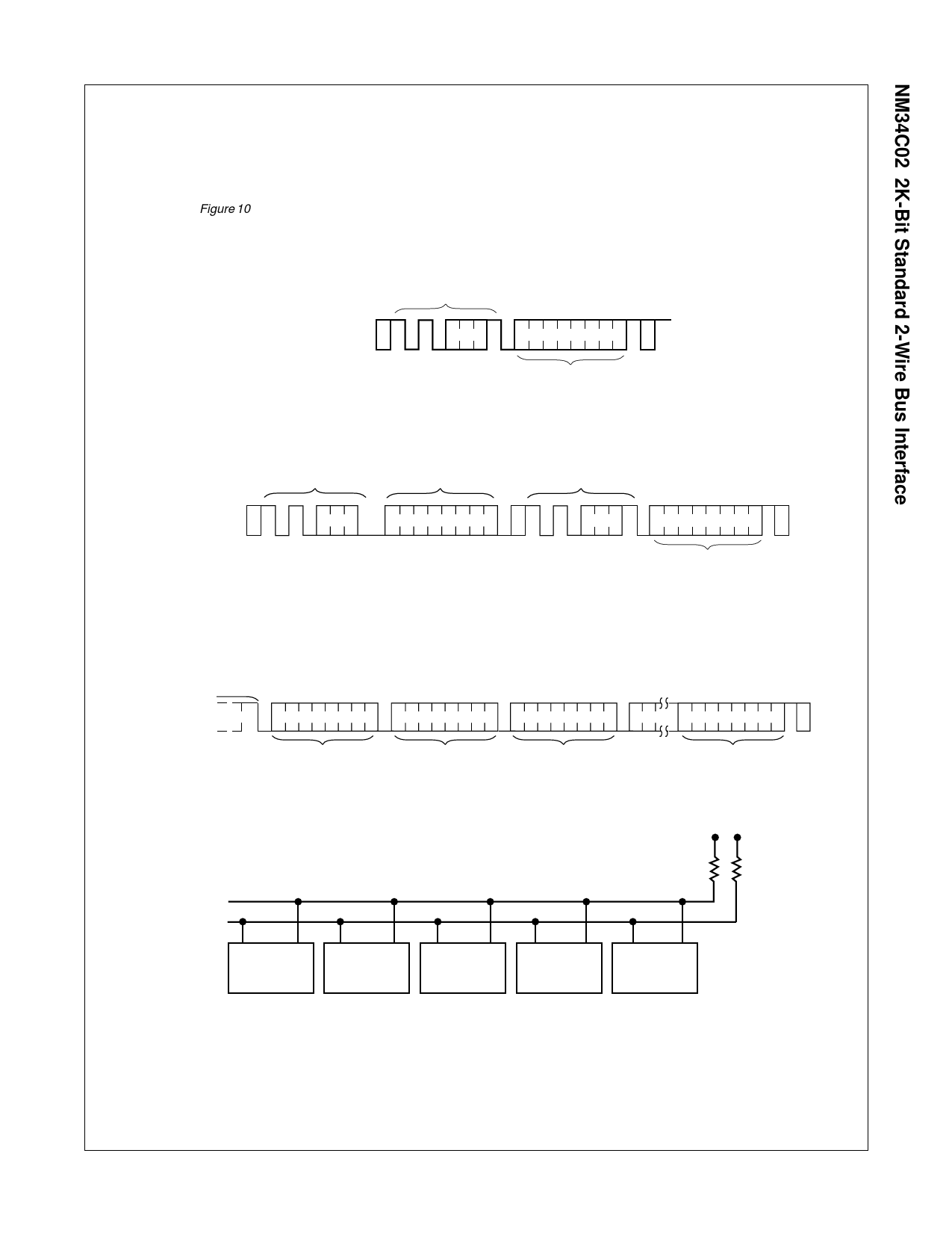
Read Operations (Continued)
operations increments all word address bits, allowing the entire
memory contents to be serially read during one operation. After
the entire memory has been read, the counter 'rolls over' and the
NM34C02 continues to output data for each acknowledge re-
ceived. Refer to Figure 10 for the address, acknowledge, and data
transfer sequence.
S
T
S
Bus Activity:
A
SLAVE
T
Master
R ADDRESS
O
T
P
SDA Line
A
C
DATA
K
Current Address Read (Figure 8).
S
T
Bus Activity: A
Master
R
T
SDA Line
SLAVE
ADDRESS
BYTE
ADDRESS
S
T
A
SLAVE
R
ADDRESS
T
S
A
A
A
C
C
C
K
K
K
Random Read (Figure 9).
DATA n
DS012821-17
S
T
O
P
DS012821-18
Bus Activity:
Master
Slave
Address
SDA Line
A
C
K
A
A
A
C
C
C
K
K
K
Data n
Data n +1
Data n + 2
Sequential Read (Figure 10).
S
T
O
P
Data n + x
DS012821-19
VCC
SDA
SCL
Master
Transmitter/
Receiver
Slave
Receiver
Slave
Transmitter/
Receiver
Master
Transmitter
Master
Transmitter/
Receiver
Note: Due to open drain configuration of SDA, a bus-level resistor is called for (Typical value = 4.7Ω)
Typical System Configuration (Figure 11).
DS012821-20
NM34C02 Rev. D.2
10
www.fairchildsemi.com
Share Link: 