NM34C02 データシートの表示(PDF) - Fairchild Semiconductor
部品番号
コンポーネント説明
一致するリスト
NM34C02 Datasheet PDF : 12 Pages
| |||
Device
NM34C02
Address Pins
A0 A1 A2
ADR ADR ADR
Memory Size
2048 Bits
Number of
Page Blocks
1
Pin Descriptions
Serial Clock (SCL)
The SCL input is used to clock all data into and out of the device.
Serial Data (SDA)
SDA is a bidirectional pin used to transfer data into and out of the
device. It is an open drain output and may be wire–ORed with any
number of open drain or open collector outputs.
Device Operation Inputs (A0, A1, A2)
Device address pins A0, A1, and A2 are connected to VCC or VSS
to configure the EEPROM chip address. Table A shows the active
pins across the NM34C02 device family.
Table 1.
Device A0 A1 A2 Effects of Addresses
NM34C02L ADR ADR ADR 8 devices max.
Device Operation
The NM34C02 supports a bidirectional bus oriented protocol. The
protocol defines any device that sends data onto the bus as a
transmitter and the receiving device as the receiver. The device
controlling the transfer is the master and the device that is
controlled is the slave. The master will always initiate data
transfers and provide the clock for both transmit and receive
operations. Therefore, the NM34C02 will be considered a slave in
all applications.
Clock and Data Conventions
Data states on the SDA line can change only during SCL LOW.
SDA state changes during SCL HIGH are reserved for indicating
start and stop conditions. Refer to Figures 1 and 2.
Start Condition
All commands are preceded by the start condition, which is a
HIGH to LOW transition of SDA when SCL is HIGH. The NM34C02
continuously monitors the SDA and SCL lines for the start condi-
tion and will not respond to any command until this condition has
been met.
Stop Condition
All communications are terminated by a stop condition, which is a
LOW to HIGH transition of SDA when SCL is HIGH. The stop
condition is also used by the NM34C02 to place the device in the
standby power mode.
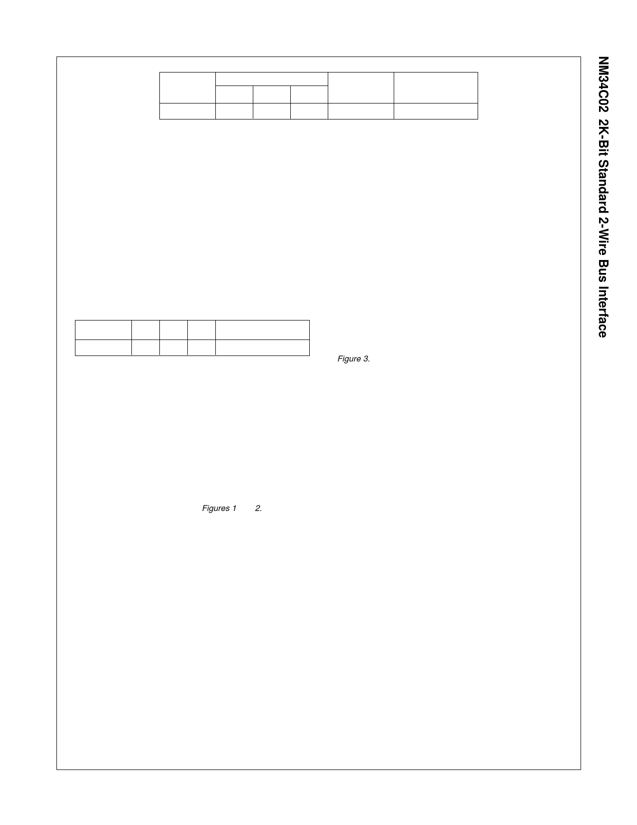
ACKNOWLEDGE
Acknowledge is a software convention used to indicate successful
data transfers. The transmitting device, either master or slave, will
release the bus after transmitting eight bits.
During the ninth clock cycle the receiver will pull the SDA line to
LOW to acknowledge that it received the eight bits of data. Refer
to Figure 3.
The NM34C02 device will always respond with an acknowledge
after recognition of a start condition and its slave address. If both
the device and a write operation have been selected, the NM34C02
will respond with an acknowledge after the receipt of each
subsequent eight bit byte.
In the Read mode the NM34C02 slave will transmit eight bits of
data, release the SDA line and monitor the line for an acknowl-
edge. If an acknowledge is detected and no stop condition is
generated by the master, the slave will continue to transmit data.
If an acknowledge is not detected, the slave will terminate further
data transmissions and await the stop condition to return to the
standby power mode.
NM34C02 Rev. D.2
6
www.fairchildsemi.com
Share Link: 