NT512D72S4PA0GR データシートの表示(PDF) - Nanya Technology
部品番号
コンポーネント説明
一致するリスト
NT512D72S4PA0GR Datasheet PDF : 14 Pages
| |||
NT512D72S4PA0GR
512MB : 64M x 72
Registered DDR SDRAM DIMM
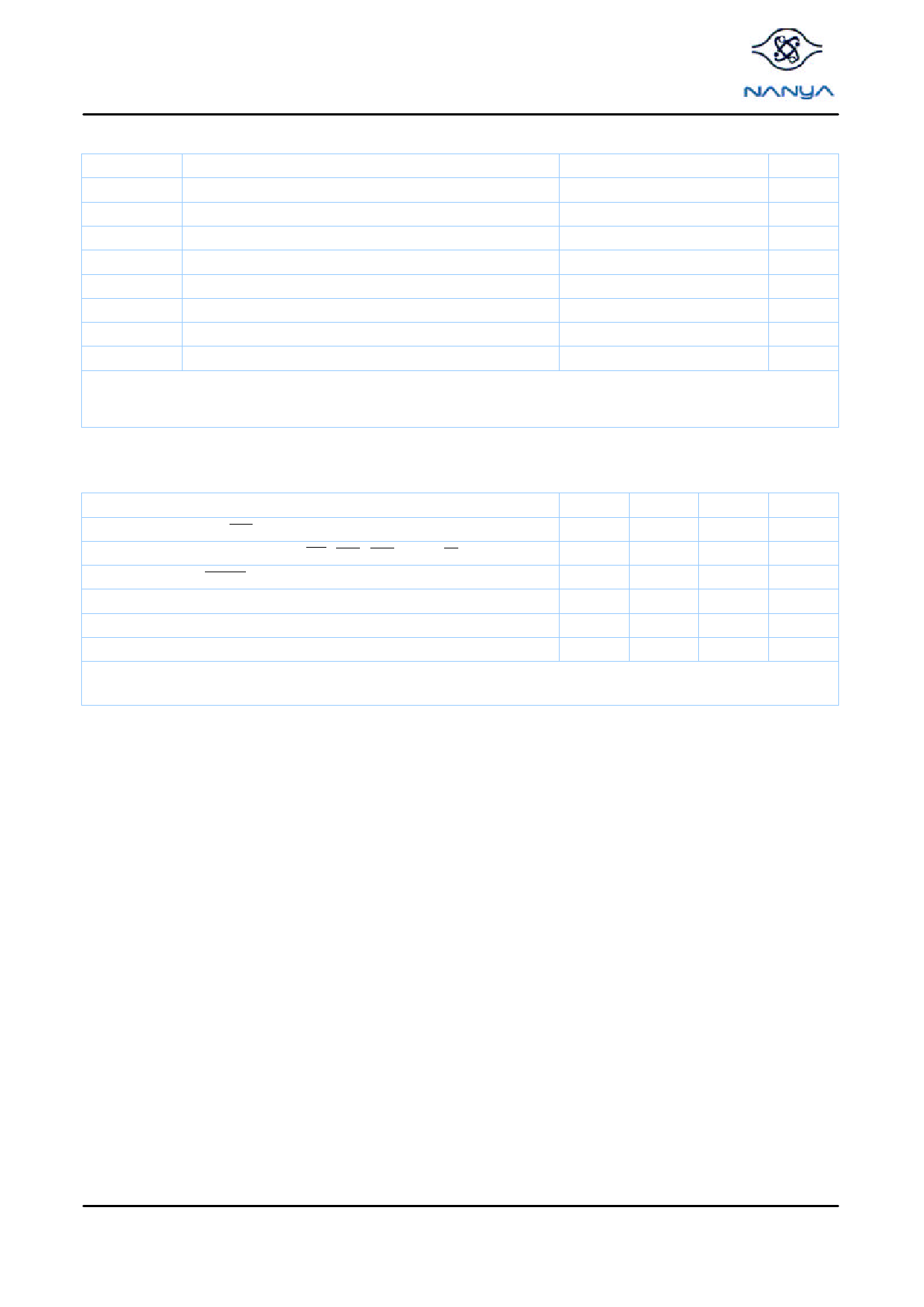
Absolute Maximum Ratings
Symbol
Parameter
Rating
Units
VIN, VOUT
Voltage on I/O pins relative to Vss
-0.5 to VDDQ+0.5
V
VIN
Voltage on Input relative to Vss
-0.5 to +2.7
V
VDD
Voltage on VDD supply relative to Vss
-0.5 to +2.7
V
VDDQ
Voltage on VDDQ supply relative to Vss
-0.5 to +2.7
V
TA
Operating Temperature (Ambient)
0 to +70
°C
TSTG
Storage Temperature (Plastic)
-55 to +150
°C
PD
Power Dissipation
18
W
IOUT
Short Circuit Output Current
50
mA
Note: Stresses greater than those listed under “Absolute Maximum Ratings” may cause permanent damage to the device. This is
stress rating only, and functional operation of the device at these or any other conditions above those indicated in the operational
sections of this specification is not implied. Exposure to absolute maximum rating conditions for extended periods may affect reliability.
Capacitance
Parameter
Symbol
Max.
Units
Notes
Input Capacitance: CK0, CK0
CI1
7
pF
1
Input Capacitance: A0-A12, BA0, BA1, WE , RAS , CAS , CKE0, S0
CI2
7
pF
1
Input Capacitance: RESET
CI3
7
pF
1
Input Capacitance: SA0-SA2, SCL
CI4
9
pF
1
Input/Output Capacitance DQ0-63; DQS0-17, CB0-7
CIO1
10
pF
1,2
Input/Output Capacitance: SDA
CIO3
11
pF
1. VDDQ = VDD = 2.5V ± 0.2V, f = 100 MHz, TA = 25 °C, VOUT (DC) = VDDQ/2, VOUT (Peak to Peak) = 0.2V.
2. DM inputs are grouped with I/O pins reflecting the fact that they are matched in loading to DQ and DQS to facilitate trace matching at
the board level.
Preliminary 08/01
7
© NANYA TECHNOLOGY CORP.
NANYA TECHNOLOGY CORP. reserves the right to change Products and Specifications without notice.
Share Link: 