NT512D72S4PA0GR データシートの表示(PDF) - Nanya Technology
部品番号
コンポーネント説明
一致するリスト
NT512D72S4PA0GR Datasheet PDF : 14 Pages
| |||
NT512D72S4PA0GR
512MB : 64M x 72
Registered DDR SDRAM DIMM
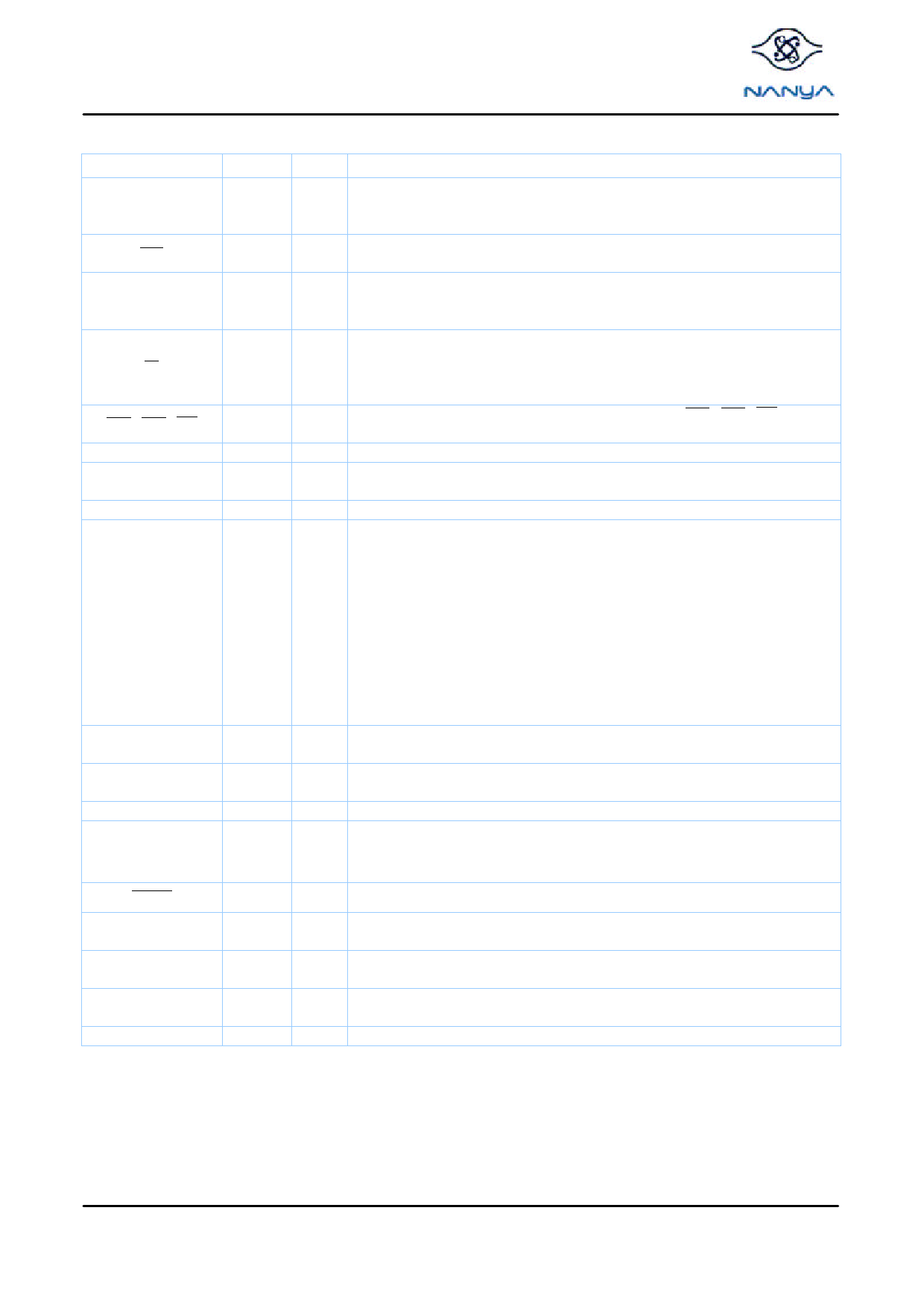
Input/Output Functional Description
Symbol
CK0
CK0
CKE0
S0
RAS , CAS , WE
VREF
VDDQ
BA0, BA1
A0 - A9
A10/AP
A11, A12
DQ0 - DQ63,
DQ0 – DQ63
CB0 – CB7
VDD , VSS
DQS0 – DQS17
RESET
SA0 – SA2
SDA
SCL
V DDSPD
Type Polarity
Function
(SSTL)
The positive line of the differential pair of system clock inputs which drives the input to
Positive
the on-DIMM PLL. All the DDR SDRAM address and control inputs are sampled on the
Edge
rising edge of their associated clocks.
Negative The negative line of the differential pair of system clock inputs which drives the input to
(SSTL)
Edge the on-DIMM PLL.
(SSTL)
Active
High
Activates the SDRAM CK signal when high and deactivates the CK signal when low. By
deactivating the clocks, CKE low initiates the Power Down mode, or the Self Refresh
mode.
Enables the associated SDRAM command decoder when low and disables the
(SSTL)
Active command
Low decoder when high. When the command decoder is disabled, new commands are
ignored but previous operations continue.
(SSTL)
Active When sampled at the positive rising edge of the clock, RAS , CAS , WE define the
Low operation to be executed by the SDRAM.
Supply
Reference voltage for SSTL-2 inputs
Supply
Isolated power supply for the DDR SDRAM output buffers to provide improved noise
immunity
(SSTL)
- Selects which SDRAM bank is to be active.
During a Bank Activate command cycle, A0-A12 defines the row address (RA0-RA12)
when sampled at the rising clock edge.
During a Read or Write command cycle, A0-A9, A11 defines the column address
(CA0-CA10) when sampled at the rising clock edge. In addition to the column address,
(SSTL)
AP is used to invoke Autoprecharge operation at the end of the Burst Read or Write
- cycle. If AP is high, autoprecharge is selected and BA0/BA1 define the bank to be
precharged. If AP is low, autoprecharge is disabled.
During a Precharge command cycle, AP is used in conjunction with BA0/BA1 to control
which bank(s) to precharge. If AP is high all 4 banks will be precharged regardless of the
state of BA0/BA1. If AP is low, then BA0/BA1 are used to define which bank to
pre-charge.
(SSTL)
-
Data and Check Bit input/output pins operate in the same manner as on conventional
DRAMs.
(SSTL)
Active Data and Check Bit Input/Output pins. Check bits are only applicable on the x72 DIMM
High configurations.
Supply
Power and ground for the DDR SDRAM input buffers and core logic
Negative
and
(SSTL) Positive Data strobe for input and output data
Edge
(LVC-MOS)
Active
Low
-
Address inputs. Connected to either VDD or VSS on the system board to configure the
Serial Presence Detect EEPROM address.
This bidirectional pin is used to transfer data into or out of the SPD EEPROM. A resistor
-
must be connected from the SDA bus line to V DD to act as a pullup.
This signal is used to clock data into and out of the SPD EEPROM. A resistor may be
-
connected from the SCL bus time to V DD to act as a pullup.
Supply
Serial EEPROM positive power supply.
Preliminary 08/01
3
© NANYA TECHNOLOGY CORP.
NANYA TECHNOLOGY CORP. reserves the right to change Products and Specifications without notice.
Share Link: 