ADSP-2191MKCA-160 データシートの表示(PDF) - Analog Devices
部品番号
コンポーネント説明
一致するリスト
ADSP-2191MKCA-160 Datasheet PDF : 52 Pages
| |||
ADSP-2191M
The two address buses (PMA and DMA) share a single external
address bus, allowing memory to be expanded off-chip, and the
two data buses (PMD and DMD) share a single external data
bus. Boot memory space and I/O memory space also share the
external buses.
Program memory can store both instructions and data, permit-
ting the ADSP-2191M to fetch two operands in a single cycle,
one from program memory and one from data memory. The
DSP’s dual memory buses also let the ADSP-219x core fetch an
operand from data memory and the next instruction from
program memory in a single cycle.
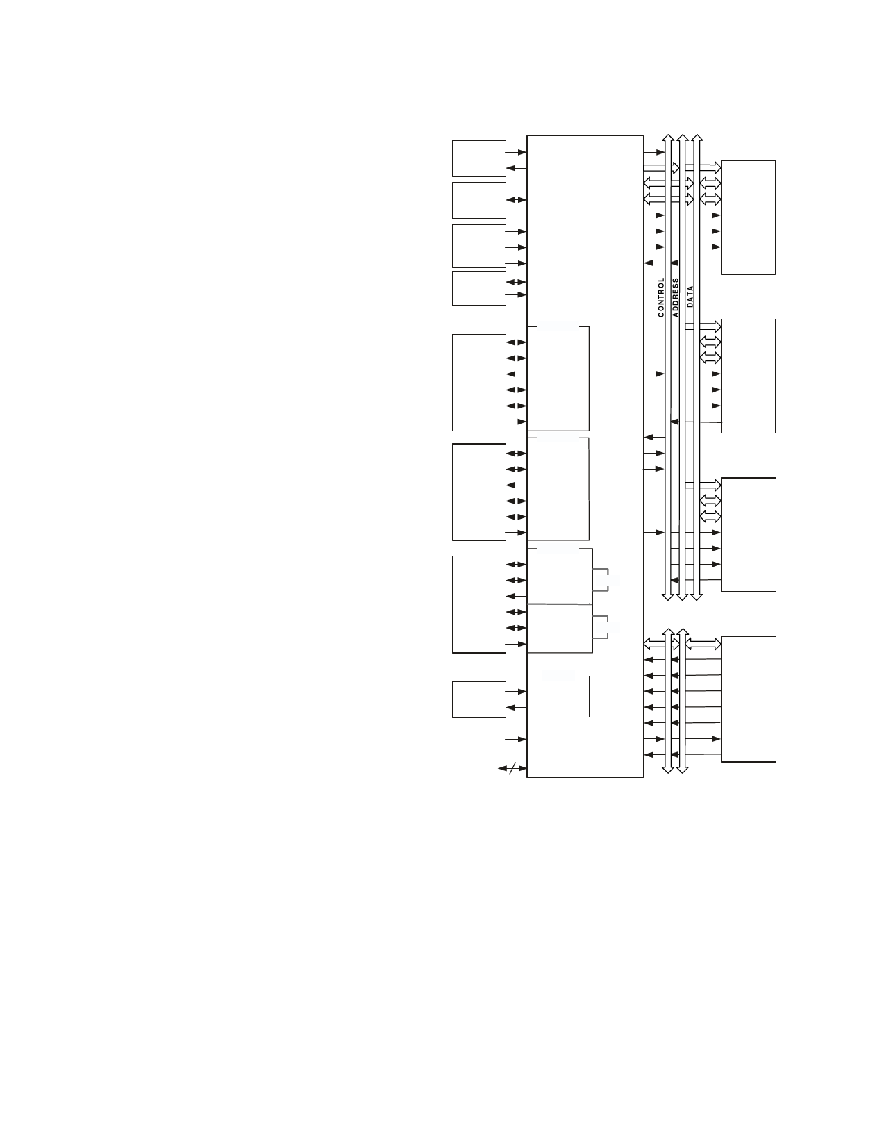
DSP Peripherals Architecture
The functional block diagram on page 1 shows the DSP’s
on-chip peripherals, which include the external memory inter-
face, Host port, serial ports, SPI-compatible ports, UART port,
JTAG test and emulation port, timers, flags, and interrupt con-
troller. These on-chip peripherals can connect to off-chip devices
as shown in Figure 1.
The ADSP-2191M has a 16-bit Host port with DMA capability
that lets external Hosts access on-chip memory. This 24-pin
parallel port consists of a 16-pin multiplexed data/address bus
and provides a low-service overhead data move capability. Con-
figurable for 8 or 16 bits, this port provides a glueless interface
to a wide variety of 8- and 16-bit microcontrollers. Two
chip-selects provide Hosts access to the DSP’s entire memory
map. The DSP is bootable through this port.
The ADSP-2191M also has an external memory interface that is
shared by the DSP’s core, the DMA controller, and DMA
capable peripherals, which include the UART, SPORT0,
SPORT1, SPORT2, SPI0, SPI1, and the Host port. The external
port consists of a 16-bit data bus, a 22-bit address bus, and
control signals. The data bus is configurable to provide an 8 or
16 bit interface to external memory. Support for word packing
lets the DSP access 16- or 24-bit words from external memory
regardless of the external data bus width. When configured for
an 8-bit interface, the unused eight lines provide eight program-
mable, bidirectional general-purpose Programmable Flag lines,
six of which can be mapped to software condition signals.
The memory DMA controller lets the ADSP-2191M move data
and instructions from between memory spaces: internal-to-exter-
nal, internal-to-internal, and external-to- external. On-chip
peripherals can also use this controller for DMA transfers.
The ADSP-2191M can respond to up to seventeen interrupts at
any given time: three internal (stack, emulator kernel, and
power-down), two external (emulator and reset), and twelve
user-defined (peripherals) interrupts. The programmer assigns a
peripheral to one of the 12 user-defined interrupts. The priority
of each peripheral for interrupt service is determined by these
assignments.
There are three serial ports on the ADSP-2191M that provide a
complete synchronous, full-duplex serial interface. This interface
includes optional companding in hardware and a wide variety of
framed or frameless data transmit and receive modes of opera-
CLOCK
OR
CRYSTAL
TIMER
OUT OR
CAPTURE
CLOCK
MULTIPLY
AND
RANGE
BOOT
AND OP
MODE
ADSP-2191M
CLKIN
CLKOUT
XTAL
ADDR21–0
DATA15–8
TMR2–0
DATA7–0
MS3–0
MSEL6–0/PF6–0
RD
DF/PF7
WR
BYPASS
ACK
BMODE1–0
OPMODE
SERIAL
DEVICE
(OP TION A L)
SERIAL
DEVICE
(O P TION A L )
SERIAL
DEVICE
(OP TION A L)
UART
DEVICE
(OP TION A L)
6
SPORT0
TCLK0
TFS0
DT0
BMS
RCLK0
RFS0
DR0
SPORT1
BR
TCLK1
BG
TFS1
BGH
DT1
RCLK1
RFS1
DR1
IOMS
SPORT2
TCLK2/SCK0
TFS2/MOSI0 SPI0
DT2/MISO0
RCLK2/SCK1
RFS2/MOSI1 SPI1
DR2/MISO1 HAD15–0
HA16
UART
HCMS
RXD
TXD
HCIOMS
HRD
HWR
RESET
HACK
JTAG
HALE
HACK_P
EXTERNAL
MEMORY
(O PTION AL)
ADDR21–0
DATA15–8
DATA7–0
CS
OE
WE
ACK
BOOT
MEMORY
(O PTION AL)
ADDR21–0
DATA15–8
DATA7–0
CS
OE
WE
ACK
EXTERNAL
I/O MEMORY
(O PTIO NAL )
ADDR17–0
DATA15–8
DATA7–0
CS
OE
WE
ACK
HOST
PROCESSOR
(O PTIO NAL )
ADDR15–0/
DATA15–0
ADDR16
CS0
CS1
RD
WR
ACK
ALE
Figure 1. System Diagram
tion. Each serial port can transmit or receive an internal or
external, programmable serial clock and frame syncs. Each serial
port supports 128-channel Time Division Multiplexing.
The ADSP-2191M provides up to sixteen general-purpose I/O
pins, which are programmable as either inputs or outputs. Eight
of these pins are dedicated-general purpose Programmable Flag
pins. The other eight of them are multifunctional pins, acting as
general-purpose I/O pins when the DSP connects to an 8-bit
external data bus and acting as the upper eight data pins when
the DSP connects to a 16-bit external data bus. These Program-
mable Flag pins can implement edge- or level-sensitive
interrupts, some of which can be used to base the execution of
conditional instructions.
–4–
REV. 0
Share Link: 