MC100EL34DG(2016) データシートの表示(PDF) - ON Semiconductor
部品番号
コンポーネント説明
一致するリスト
MC100EL34DG Datasheet PDF : 9 Pages
| |||
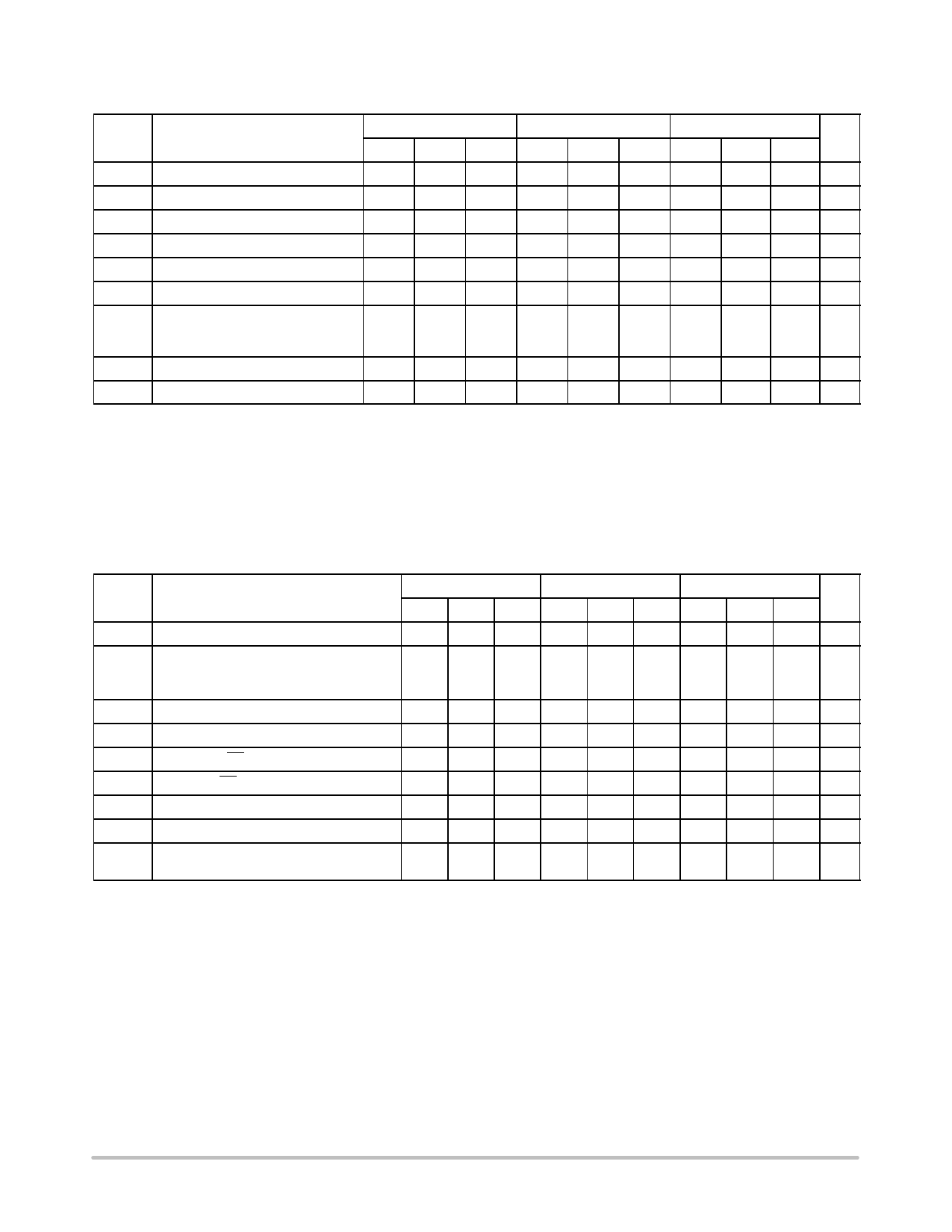
MC10EL34, MC100EL34
Table 8. 100EL SERIES NECL DC CHARACTERISTICS (VCC = 0 V; VEE = −5.0 V (Note 1))
−40°C
25°C
85°C
Symbol
Characteristic
Min Typ Max Min Typ Max Min Typ Max Unit
IEE Power Supply Current
39
39
42 mA
VOH Output HIGH Voltage (Note 2)
−1085 −1005 −880 −1025 −955 −880 −1025 −955 −880 mV
VOL Output LOW Voltage (Note 2)
−1830 −1695 −1555 −1810 −1705 −1620 −1810 −1705 −1620 mV
VIH Input HIGH Voltage (Single-Ended) −1165
−880 −1165
−880 −1165
−880 mV
VIL Input LOW Voltage (Single-Ended) −1810
−1475 −1810
−1475 −1810
−1475 mV
VBB Output Voltage Reference
−1.38
−1.26 −1.38
−1.26 −1.38
−1.26 V
VIHCMR Input HIGH Voltage Common Mode −2.8
Range (Differential Configuration)
(Note 3)
−0.4 −2.8
−0.4 −2.8
−0.4 V
IIH
Input HIGH Current
IIL
Input LOW Current
150
150
150 mA
0.5
0.5
0.5
mA
NOTE: Device will meet the specifications after thermal equilibrium has been established when mounted in a test socket or printed circuit
board with maintained transverse airflow greater than 500 lfpm. Electrical parameters are guaranteed only over the declared
operating temperature range. Functional operation of the device exceeding these conditions is not implied. Device specification limit
values are applied individually under normal operating conditions and not valid simultaneously.
1. Input and output parameters vary 1:1 with VCC. VEE can vary +0.8 V / −0.5 V.
2. Outputs are terminated through a 50ĂW resistor to VCC − 2.0 V.
3. VIHCMR min varies 1:1 with VEE, VIHCMR max varies 1:1 with VCC. The VIHCMR range is referenced to the most positive side of the differential input
signal. Normal operation is obtained if the HIGH level falls within the specified range and the peak-to-peak voltage lies between VPPmin and 1 V.
Table 9. AC CHARACTERISTICS (VCC = 5.0 V; VEE = 0.0 V or VCC = 0.0 V; VEE = −5.0 V (Note 1))
−40°C
25°C
85°C
Symbol
Characteristic
fmax Maximum Toggle Frequency
Min Typ Max Min Typ Max Min Typ Max Unit
1.1
1.1
1.1
GHz
tPLH Propagation
tPHL
CLK to Q0
Delay to
CLK to Q1,2
Output
MR to Q
ps
960
1200 960
1200 970
1210
900
1140 900
1140 910
1150
750
1060 750
1060 790
1090
tSKEW
tJITTER
tS
tH
tRR
VPP
tr
tf
Within-Device Skew (Note 2)
Cycle-to-Cycle Jitter
Setup Time EN
Hold Time EN
Set/Reset Recovery
Input Swing (Note 3)
Output Rise/Fall Times Q
(20% − 80%)
100
100
100
ps
1.0
1.0
1.0
ps
400
400
400
ps
250
250
250
ps
400 200
400 200
400 200
ps
150
1000 150
1000 150
1000 mV
225
475 225
475 225
475 ps
NOTE: Device will meet the specifications after thermal equilibrium has been established when mounted in a test socket or printed circuit
board with maintained transverse airflow greater than 500 lfpm. Electrical parameters are guaranteed only over the declared
operating temperature range. Functional operation of the device exceeding these conditions is not implied. Device specification limit
values are applied individually under normal operating conditions and not valid simultaneously.
1. 10 Series: VEE can vary +0.06 V / −0.5 V.
100 Series: VEE can vary +0.8 V / −0.5 V.
2. Within-device skew is defined as identical transitions on similar paths through a device.
3. VPPmin is minimum input swing for which AC parameters guaranteed. The device has a DC gain of ≈40.
www.onsemi.com
5
Share Link: 