MC100EL34DG(2016) データシートの表示(PDF) - ON Semiconductor
部品番号
コンポーネント説明
一致するリスト
MC100EL34DG Datasheet PDF : 9 Pages
| |||
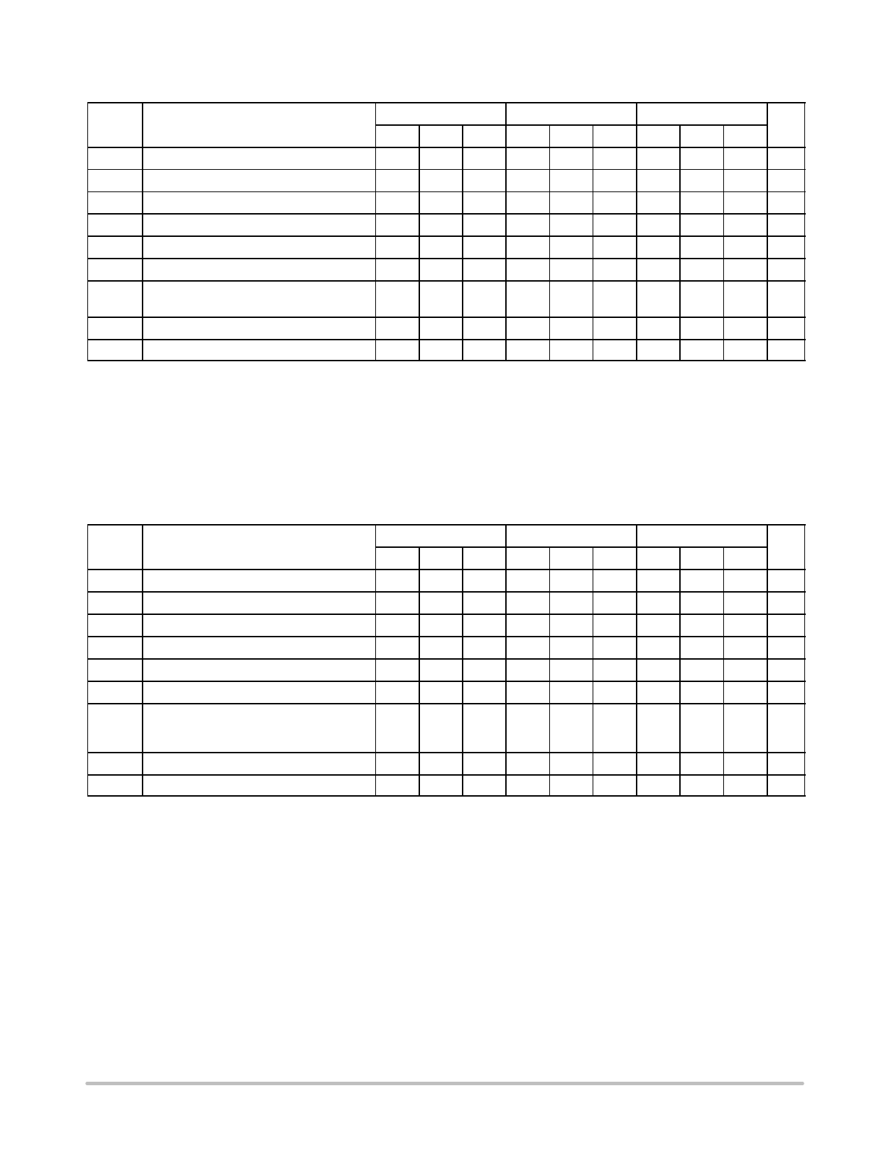
MC10EL34, MC100EL34
Table 6. 10EL SERIES NECL DC CHARACTERISTICS (VCC = 0 V; VEE = −5.0 V (Note 1))
−40°C
25°C
85°C
Symbol
Characteristic
IEE Power Supply Current
VOH Output HIGH Voltage (Note 2)
VOL Output LOW Voltage (Note 2)
VIH Input HIGH Voltage (Single-Ended)
VIL Input LOW Voltage (Single-Ended)
VBB Output Voltage Reference
VIHCMR Input HIGH Voltage Common Mode
Range (Differential) (Note 3)
Min Typ Max Min Typ Max Min Typ Max Unit
39
39
39 mA
−1080 −990 −890 −980 −895 −810 −910 −815 −720 mV
−1950 −1800 −1650 −1950 −1790 −1630 −1950 −1773 −1595 mV
−1230
−890 −1130
−810 −1060
−720 mV
−1950
−1500 −1950
−1480 −1950
−1445 mV
−1.43
−1.30 −1.35
−1.25 −1.31
−1.19 V
−2.0
−0.4 −2.0
−0.4 −2.0
−0.4 V
IIH
Input HIGH Current
150
150
150 mA
IIL
Input LOW Current
0.5
0.5
0.3
mA
NOTE: Device will meet the specifications after thermal equilibrium has been established when mounted in a test socket or printed circuit
board with maintained transverse airflow greater than 500 lfpm. Electrical parameters are guaranteed only over the declared
operating temperature range. Functional operation of the device exceeding these conditions is not implied. Device specification limit
values are applied individually under normal operating conditions and not valid simultaneously.
1. Input and output parameters vary 1:1 with VCC. VEE can vary +0.06 V / −0.5 V.
2. Outputs are terminated through a 50ĂW resistor to VCC − 2.0 V.
3. VIHCMR min varies 1:1 with VEE, VIHCMR max varies 1:1 with VCC. The VIHCMR range is referenced to the most positive side of the differential input
signal. Normal operation is obtained if the HIGH level falls within the specified range and the peak-to-peak voltage lies between VPPmin and 1 V.
Table 7. 100EL SERIES PECL DC CHARACTERISTICS (VCC = 5.0 V; VEE = 0 V (Note 1))
−40°C
25°C
85°C
Symbol
Characteristic
IEE Power Supply Current
VOH Output HIGH Voltage (Note 2)
VOL Output LOW Voltage (Note 2)
VIH Input HIGH Voltage (Single-Ended)
VIL Input LOW Voltage (Single-Ended)
VBB Output Voltage Reference
VIHCMR Input HIGH Voltage Common Mode
Range (Differential Configuration) (Note 3)
Min
3915
3170
3835
3190
3.62
2.2
Typ
3995
3305
Max
39
4120
3445
4120
3525
3.74
4.6
Min
3975
3190
3835
3190
3.62
2.2
Typ
4045
3295
Max
39
4120
3380
4120
3525
3.74
4.6
Min
3975
3190
3835
3190
3.62
2.2
Typ
4050
3295
Max Unit
42 mA
4120 mV
3380 mV
4120 mV
3525 mV
3.74 V
4.6 V
IIH
Input HIGH Current
150
150
150 mA
IIL
Input LOW Current
0.5
0.5
0.5
mA
NOTE: Device will meet the specifications after thermal equilibrium has been established when mounted in a test socket or printed circuit
board with maintained transverse airflow greater than 500 lfpm. Electrical parameters are guaranteed only over the declared
operating temperature range. Functional operation of the device exceeding these conditions is not implied. Device specification limit
values are applied individually under normal operating conditions and not valid simultaneously.
1. Input and output parameters vary 1:1 with VCC. VEE can vary +0.8 V / −0.5 V.
2. Outputs are terminated through a 50ĂW resistor to VCC − 2.0 V.
3. VIHCMR min varies 1:1 with VEE, VIHCMR max varies 1:1 with VCC. The VIHCMR range is referenced to the most positive side of the differential input
signal. Normal operation is obtained if the HIGH level falls within the specified range and the peak-to-peak voltage lies between VPPmin and 1 V.
www.onsemi.com
4
Share Link: 