MC100EL34DG(2016) データシートの表示(PDF) - ON Semiconductor
部品番号
コンポーネント説明
一致するリスト
MC100EL34DG Datasheet PDF : 9 Pages
| |||
MC10EL34, MC100EL34
5 V ECL P2, P4, P8 Clock
Generation Chip
Description
The MC10/100EL34 is a low skew ÷2, ÷4, ÷8 clock generation chip
designed explicitly for low skew clock generation applications. The
internal dividers are synchronous to each other, therefore, the common
output edges are all precisely aligned. The VBB pin, an internally
generated voltage supply, is available to this device only. For
single-ended input conditions, the unused differential input is
connected to VBB as a switching reference voltage. VBB may also
rebias AC coupled inputs. When used, decouple VBB and VCC via a
0.01 mF capacitor and limit current sourcing or sinking to 0.5 mA.
When not used, VBB should be left open.
The common enable (EN) is synchronous so that the internal
dividers will only be enabled/disabled when the internal clock is
already in the LOW state. This avoids any chance of generating a runt
clock pulse on the internal clock when the device is enabled/disabled
as can happen with an asynchronous control. An internal runt pulse
could lead to losing synchronization between the internal divider
stages. The internal enable flip−flop is clocked on the falling edge of
the input clock, therefore, all associated specification limits are
referenced to the negative edge of the clock input.
Upon startup, the internal flip-flops will attain a random state; the
master reset (MR) input allows for the synchronization of the internal
dividers, as well as multiple EL34s in a system.
The 100 Series contains temperature compensation.
Features
• 50 ps Output-to-Output Skew
• Synchronous Enable/Disable
• Master Reset for Synchronization
• PECL Mode Operating Range:
♦ VCC = 4.2 V to 5.7 V with VEE = 0 V
• NECL Mode Operating Range:
♦ VCC = 0 V with VEE = −4.2 V to −5.7 V
• Internal Input 75 kW Pulldown Resistors on CLK(s), EN, and MR
• These Devices are Pb-Free, Halogen Free and are RoHS Compliant
www.onsemi.com
16
1
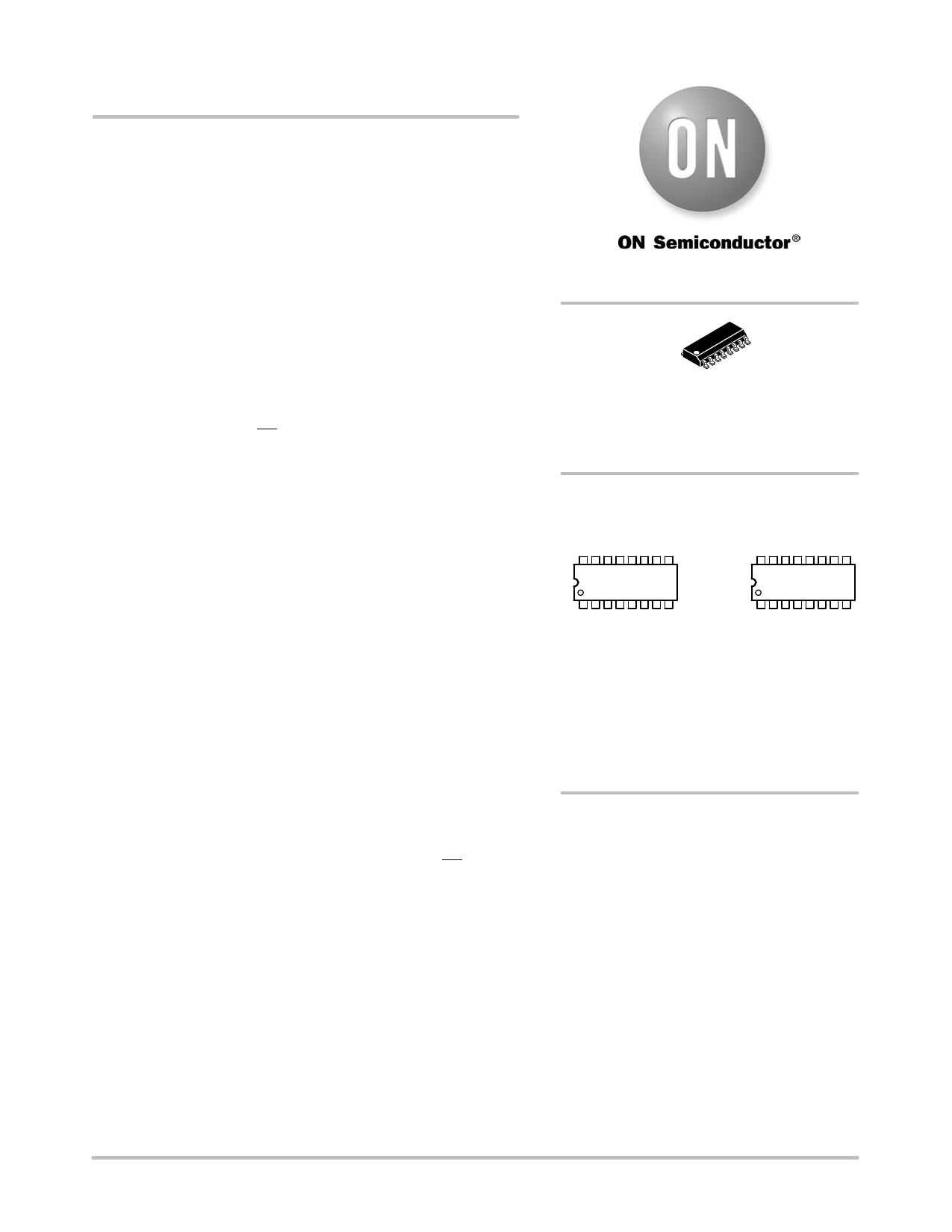
SOIC−16
D SUFFIX
CASE 751B−05
MARKING DIAGRAMS*
16
10EL34G
AWLYWW
1
16
100EL34G
AWLYWW
1
A
= Assembly Location
WL = Wafer Lot
YY
= Year
WW = Work Week
G
= Pb-Free Package
*For additional marking information, refer to
Application Note AND8002/D.
ORDERING INFORMATION
Device
MC10EL34DG
MC100EL34DG
Package
SOIC−16
Pb-Free)
SOIC−16
(Pb-Free)
Shipping
48 Units/Tube
48 Units/Tube
© Semiconductor Components Industries, LLC, 2016
1
July, 2016 − Rev. 11
Publication Order Number:
MC10EL34/D
Share Link: 