MC100EL34DG(2016) データシートの表示(PDF) - ON Semiconductor
部品番号
コンポーネント説明
一致するリスト
MC100EL34DG Datasheet PDF : 9 Pages
| |||
MC10EL34, MC100EL34
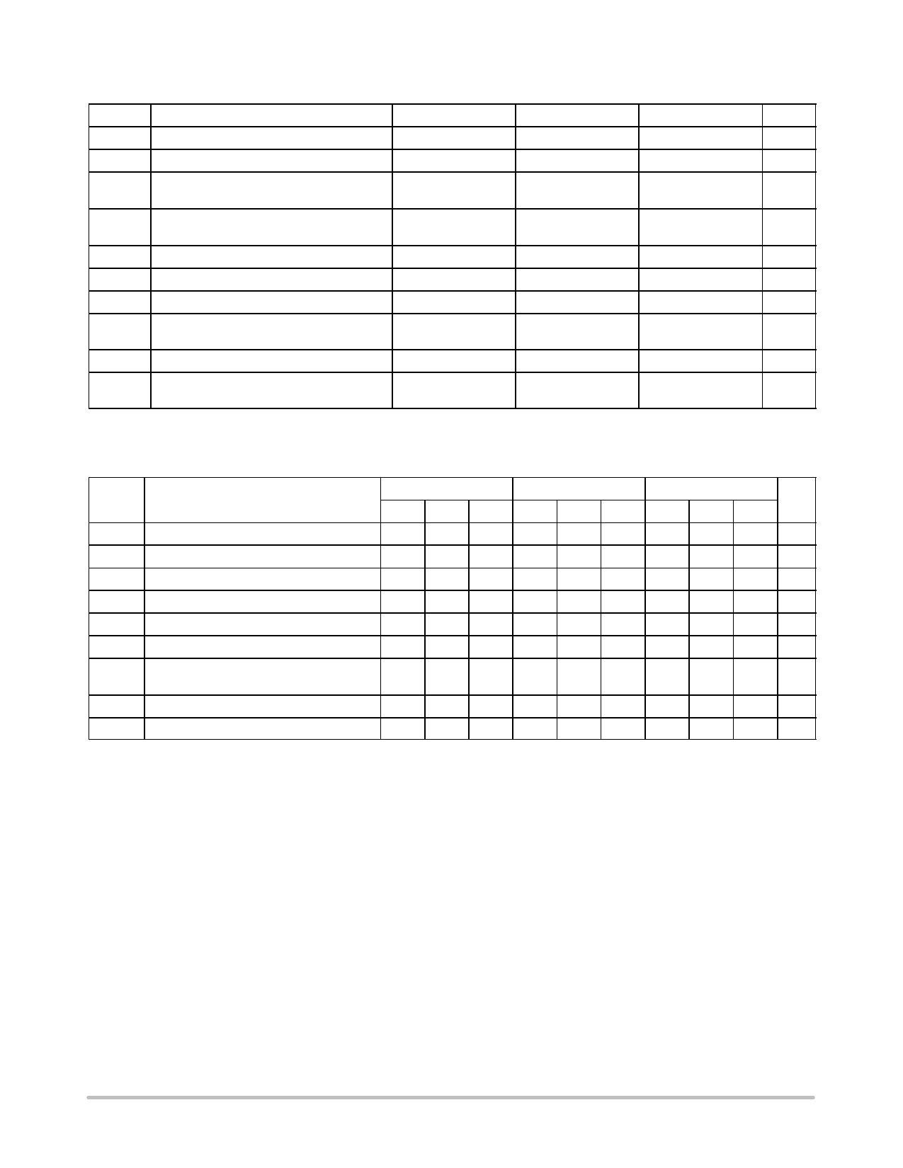
Table 4. MAXIMUM RATINGS
Symbol
Parameter
Condition 1
Condition 2
Rating
Unit
VCC PECL Mode Power Supply
VEE
NECL Mode Power Supply
VI
PECL Mode Input Voltage
NECL Mode Input Voltage
Iout
Output Current
VEE = 0 V
VCC = 0 V
VEE = 0 V
VCC = 0 V
Continuous
Surge
VI ≤ VCC
VI ≥ VEE
8
V
−8
V
6
V
−6
50
mA
100
IBB
VBB Sink/Source
TA
Operating Temperature Range
Tstg
Storage Temperature Range
qJA
Thermal Resistance (Junction-to-Ambient) 0 lfpm
500 lfpm
SOIC−16
± 0.5
−40 to +85
−65 to +150
130
75
mA
°C
°C
°C/W
qJC
Thermal Resistance (Junction-to-Case)
Tsol
Wave Solder (Pb-Free)
Standard Board
SOIC−16
<2 to 3 sec @ 260°C
33 to 36
265
°C/W
°C
Stresses exceeding those listed in the Maximum Ratings table may damage the device. If any of these limits are exceeded, device functionality
should not be assumed, damage may occur and reliability may be affected.
Table 5. 10EL SERIES PECL DC CHARACTERISTICS (VCC = 5.0 V; VEE = 0 V (Note 1))
−40°C
25°C
85°C
Symbol
Characteristic
IEE Power Supply Current
VOH Output HIGH Voltage (Note 2)
VOL Output LOW Voltage (Note 2)
VIH Input HIGH Voltage (Single-Ended)
VIL Input LOW Voltage (Single-Ended)
VBB Output Voltage Reference
VIHCMR Input HIGH Voltage Common Mode
Range (Differential) (Note 3)
Min
3920
3050
3770
3050
3.57
3.0
Typ
4010
3200
Max
39
4110
3350
4110
3500
3.7
4.6
Min
4020
3050
3870
3050
3.65
3.0
Typ
4105
3210
Max
39
4190
3370
4190
3520
3.75
4.6
Min
4090
3050
3940
3050
3.69
3.0
Typ
4185
3227
Max Unit
39 mA
4280 mV
3405 mV
4280 mV
3555 mV
3.81 V
4.6 V
IIH
Input HIGH Current
150
150
150 mA
IIL
Input LOW Current
0.5
0.5
0.3
mA
NOTE: Device will meet the specifications after thermal equilibrium has been established when mounted in a test socket or printed circuit
board with maintained transverse airflow greater than 500 lfpm. Electrical parameters are guaranteed only over the declared
operating temperature range. Functional operation of the device exceeding these conditions is not implied. Device specification limit
values are applied individually under normal operating conditions and not valid simultaneously.
1. Input and output parameters vary 1:1 with VCC. VEE can vary +0.06 V / −0.5 V.
2. Outputs are terminated through a 50 W resistor to VCC − 2.0 V.
3. VIHCMR min varies 1:1 with VEE, VIHCMR max varies 1:1 with VCC. The VIHCMR range is referenced to the most positive side of the differential input
signal. Normal operation is obtained if the HIGH level falls within the specified range and the peak-to-peak voltage lies between VPPmin and 1 V.
www.onsemi.com
3
Share Link: 