7C185A-20 データシートの表示(PDF) - Cypress Semiconductor
部品番号
コンポーネント説明
一致するリスト
7C185A-20 Datasheet PDF : 10 Pages
| |||
CY7C185A
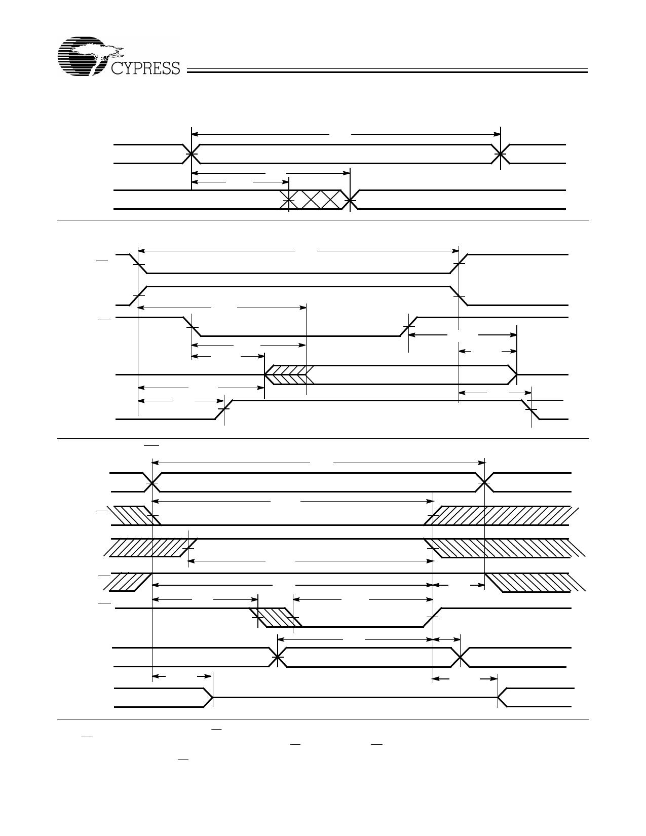
Switching Waveforms
Read Cycle No. 1[10, 11]
tRC
ADDRESS
DATA OUT
tAA
tOHA
PREVIOUS DATA VALID
Read Cycle No. 2[11, 12]
tRC
CE1
CE2
OOEE
DATA OUT
VCC
SUPPLY
CURRENT
tACE
tDOE
tLZOE
HIGH IMPEDANCE
tLZCE
tPU
50%
DATA VALID
Write Cycle No. 1 (WE Controlled)[13, 14]
ADDRESS
CE1
tWC
tSCE1
CE2
OE
WE
tSCE2
tAW
tSA
tPWE
DATA VALID
C185A–6
tHZOE
tHZCE
HIGH
IMPEDANCE
tPD
50%
ICC
ISB
C185A–7
tHA
DATA IN
tSD
tHD
DATAIN VALID
DATA I/O
tHZOE
DATA UNDEFINED
HIGH IMPEDANCE
tLZWE
C185A–8
Notes:
11. Address valid prior to or coincident with CE transition LOW.
12. WE is HIGH for read cycle.
13. The internal write time of the memory is defined by the overlap of CE1 LOW, CE2 HIGH, and WE LOW. Both signals must be LOW to initiate a write and either signal
can terminate a write by going HIGH. The data input set-up and hold timing should be referenced to the rising edge of the signal that terminates the write.
14. Data I/O is high impedance if OE = VIH.
5
Share Link: 