7C185A-20 データシートの表示(PDF) - Cypress Semiconductor
部品番号
コンポーネント説明
一致するリスト
7C185A-20 Datasheet PDF : 10 Pages
| |||
CY7C185A
Features
• High speed
— 20 ns
• CMOS for optimum speed/power
• Low active power
— 743 mW
• Low standby Power
— 220 mW
• TTL-compatible inputs and outputs
• Easy memory expansion with CE1, CE2 and OE features
• Automatic power-down when deselected
Functional Description
The CY7C185A is a high-performance CMOS static RAM or-
ganized as 8192 words by 8 bits. Easy memory expansion is
provided by an active LOW Chip Enable (CE1), an active HIGH
Chip Enable (CE2), an active LOW Output Enable (OE), and
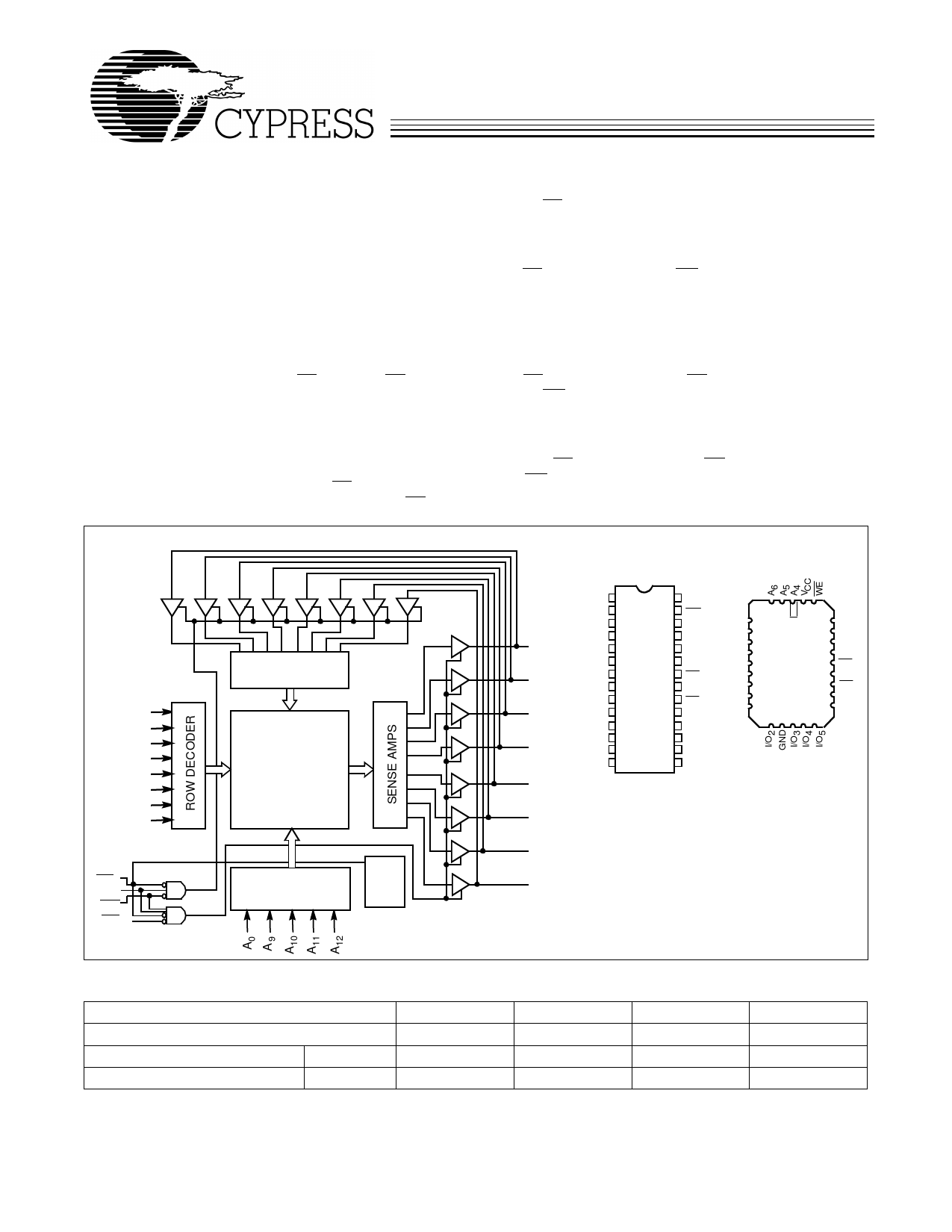
Logic Block Diagram
A1
A2
A3
A4
A5
A6
A7
A8
CE1
CE2
WE
OE
INPUT BUFFER
8K x 8
ARRAY
POWER
COLUMN DECODER DOWN
8K x 8 Static RAM
three-state drivers. The device has an automatic power-down
feature (CE1), reducing the power consumption by over 70%
when deselected. The CY7C185A is in the standard
300-mil-wide DIP package and leadless chip carrier.
Writing to the device is accomplished when the Chip Enable
one (CE1) and Write Enable (WE) inputs are both LOW, and
the Chip Enable two (CE2) input is HIGH.
Data on the eight I/O pins (I/O0 through I/O7) is written into the
memory location specified on the address pins (A0 through
A12).
Reading the device is accomplished by taking Chip Enable
one (CE1) and Output Enable (OE) LOW, while taking Write
Enable (WE) and Chip Enable two (CE2) HIGH. Under these
conditions, the contents of the memory location specified on
the address pins will appear on the I/O pins.
The I/O pins remain in a high-impedance state when Chip En-
able one (CE1) or Output Enable (OE) is HIGH, or Write En-
able (WE) or Chip Enable two (CE2) is LOW.
A die coat is used to ensure alpha immunity.
Pin Configurations
DIP
Top View
LCC
Top View
I/O0
I/O1
I/O2
I/O3
I/O4
NC 1
A4 2
A5 3
A6 4
A7 5
A8 6
A9 7
A10 8
A11 9
A12 10
I/O0 11
I/O1 12
I/O2 13
GND 14
28 VCC
27 WE
26 CE2
25 A3
24 A2
23 A1
22 OE
21 A0
20 CE1
19 I/O7
18 I/O6
17 I/O5
16 I/O4
15 I/O3
C185A–2
3 2 1 2827
NC 4
26 CE2
A7 5
25 A3
A8 6
A9 7
A10 8
24 A2
23 A1
22 OE
A11 9
21 A0
A12 10
20 CE1
I/O0 11
19 I/O7
I/O1 12
18 I/O6
1314151617
C185A–3
I/O5
I/O6
I/O7
C185A–1
Selection Guide[1]
7C185A–20
Maximum Access Time (ns)
Maximum Operating Current (mA) Military
Maximum Standby Current (mA) Military
Note:
1. For commercial specifications, see the CY7C185 data sheet.
20
135
40/20
7C185A–25
25
125
40/20
7C185A–35
35
125
30/20
7C185A–45
45
125
30/20
Cypress Semiconductor Corporation • 3901 North First Street • San Jose • CA 95134 • 408-943-2600
October 4, 1999
Share Link: 