ADSP-2191MKCA-160X データシートの表示(PDF) - Analog Devices
部品番号
コンポーネント説明
一致するリスト
ADSP-2191MKCA-160X Datasheet PDF : 66 Pages
| |||
35(/,0,1$5< 7(&+1,&$/ '$7$
September 2001 For current information contact Analog Devices at 800/262-5643
ADSP-2191
,1 7 ( 5 1 $ /
0(025<
(;7(51$/
0(025<
%,7
,1 7 ( 5 1 $ /
0(025<
. : 25'
0(025<
3$*(6
3$*(
5(6(59('
%227 520 %,7
$''5(66
[)) ))))
[)) )
[))
3$*(6
±
%$1 .
06
[&
3$*(6 ±
3$*(6 ±
%$1 .
06
%$1 .
06
[
[
3$*(6 ±
3$*(
%$1 .
06
[
%/2&. %,7 [
%/2&. %,7 [
/2:(5 3$*( %281'$5,(6
$5( &21),*85$%/( )25
%$1.6 2) (;7(51$/ 0(025<
%281'$5,(6 6+2:1 $5(
%$1. 6,=(6 $7 5(6(7
$''5(66
[)( ))))
0(025< 6(/(&76 06
)25 3257,216 2) 7+(
0(025< 0$3 $33($5
:,7+ 7+( 6(/(&7('
0(025<
%227
0(025<
%,7
%06
. : 25'
3$*(6 ±
[
,2 0(025<
%,7
. :25'
3$*(6 ±
. :25'
3$*(6 ±
(;7(51$/
,2 0 6
,17(51$/
$''5(66
[ ))))
[
[
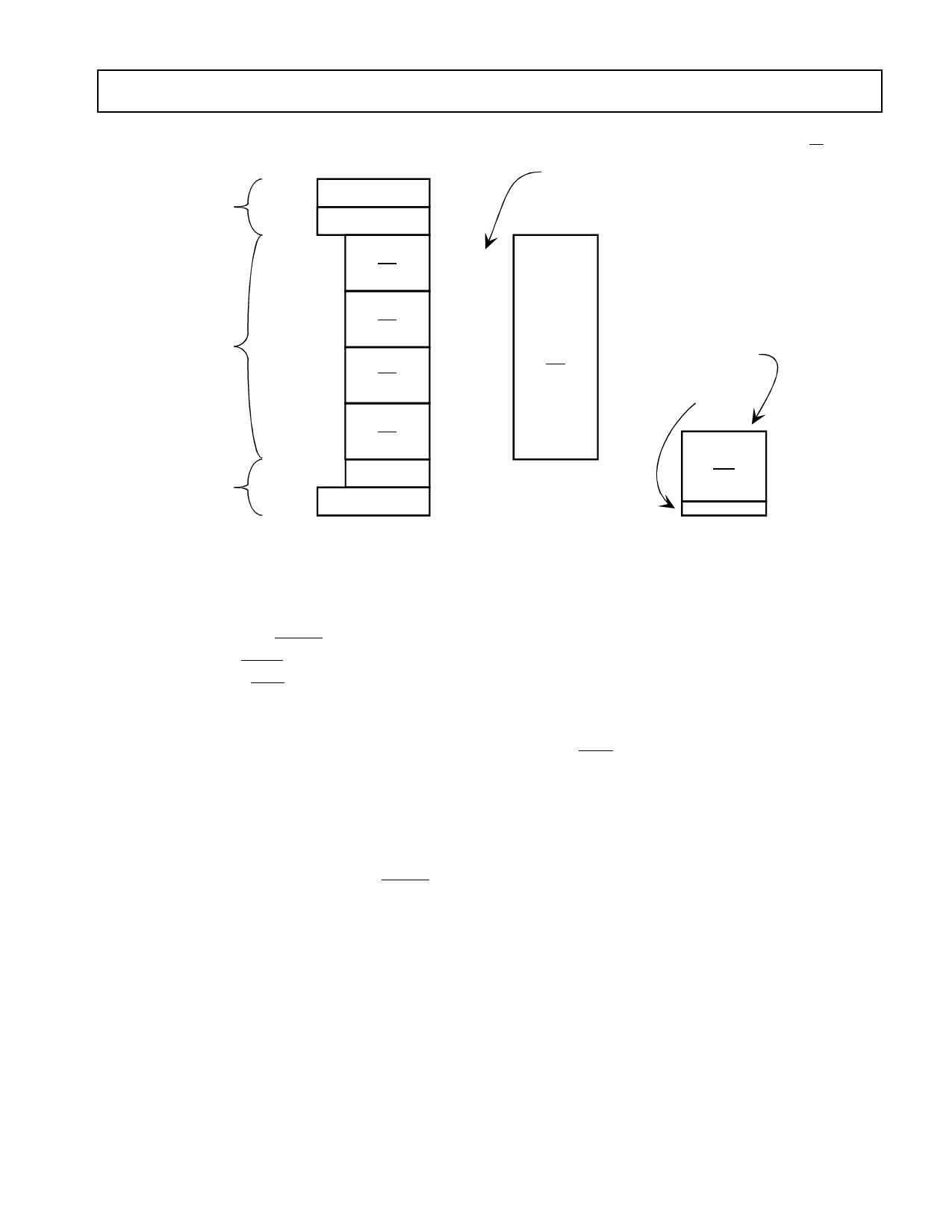
Figure 2. ADSP-2191 Memory Map
clock and peripheral clock ratios influence the external
memory access strobe widths. For more information, see
Clock Signals on page 13. The off-chip memory spaces are:
• External memory space (MS3–0 pins)
• I/O memory space (IOMS pin)
• Boot memory space (BMS pin)
All of these off-chip memory spaces are accessible through
the External Port, which can be configured for 8-bit or
16-bit data widths.
External Memory Space
External memory space consists of four memory banks.
These banks can contain a configurable number of 64K
word pages. At reset, the page boundaries for external
memory have Bank0 containing pages 1−63, Bank1 con-
taining pages 64−127, Bank2 containing pages 128−191,
and Bank3 containing Pages 192−254. The MS3–0
memory bank pins select Banks 3–0, respectively. The
external memory interface decodes the 8 MSBs of the DSP
program address to select one of the four banks. Both the
ADSP-219x core and DMA-capable peripherals can access
the DSP’s external memory space.
I/O Memory Space
The ADSP-2191 supports an additional external memory
called I/O memory space. This space is designed to support
simple connections to peripherals (such as data converters
and external registers) or to bus interface ASIC data regis-
ters. I/O space supports a total of 256K locations. The first
8K addresses are reserved for on-chip peripherals. The
upper 248K addresses are available for external peripheral
devices. The DSP’s instruction set provides instructions for
accessing I/O space. These instructions use an 18-bit
address that is assembled from an 8-bit I/O page (IOPG)
register and a 10-bit immediate value supplied in the
instruction. Both the ADSP-219x core and a Host (through
the Host Port Interface) can access I/O memory space.
Boot Memory Space
Boot memory space consists of one off-chip bank with 254
pages. The BMS memory bank pin selects boot memory
space. Both the ADSP-219x core and DMA-capable
peripherals can access the DSP’s off-chip boot memory
space. After reset, the DSP always starts executing instruc-
tions from the on-chip boot ROM. Depending on the boot
configuration, the boot ROM code can start booting the
DSP from boot memory. For more information, see Booting
Modes on page 14.
REV. PrC
This information applies to a product under development. Its characteristics and specifications are subject to change with-
7
out notice. Analog Devices assumes no obligation regarding future manufacturing unless otherwise agreed to in writing.
Share Link: 