IMIC9835 データシートの表示(PDF) - Cypress Semiconductor
部品番号
コンポーネント説明
一致するリスト
IMIC9835
Cypress Semiconductor

IMIC9835 Datasheet PDF : 18 Pages
| |||
C9835
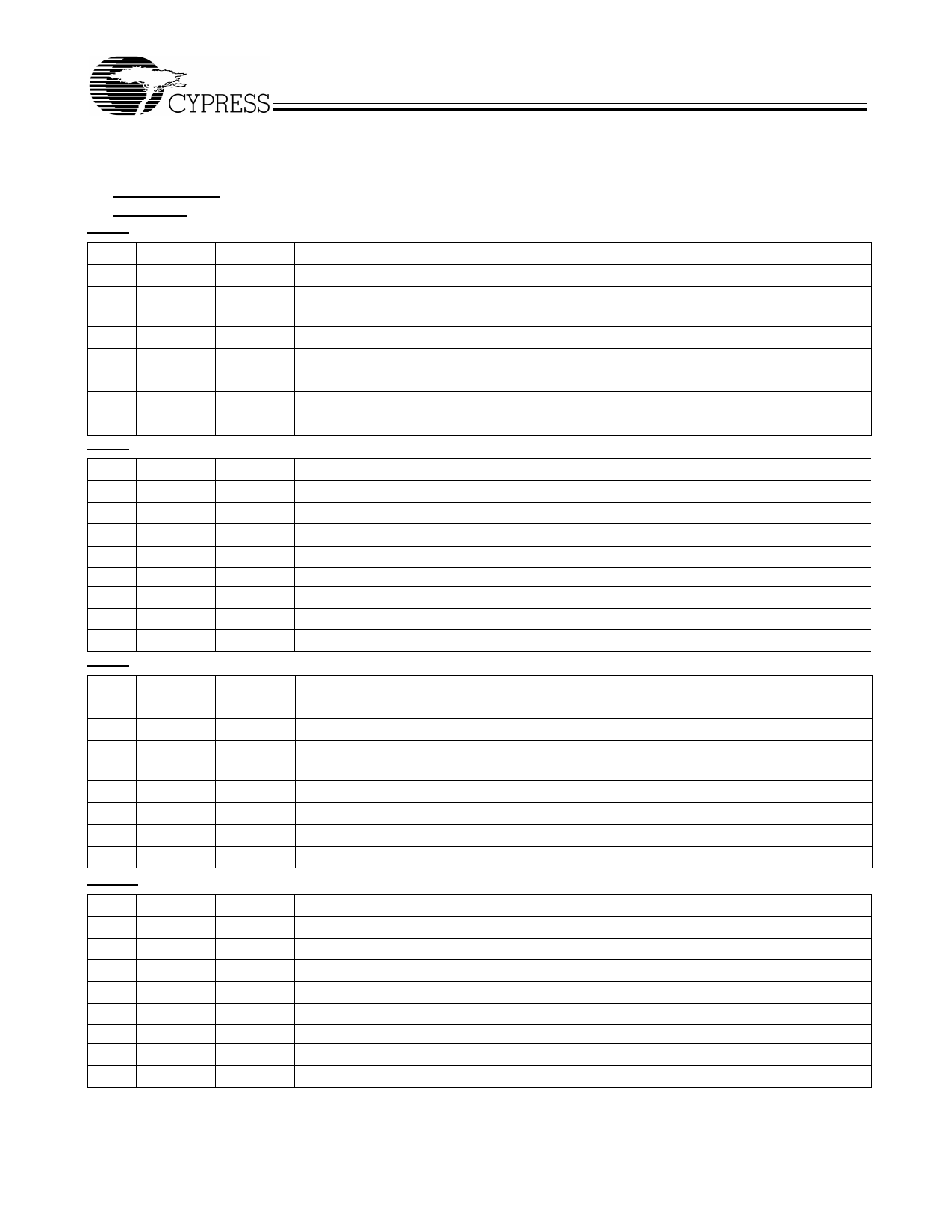
Serial Control Registers
Following the acknowledge of the Address Byte, two additional
bytes must be sent:
1) “Command Code “ byte
2) “Byte Count” byte.
Byte 0: CPU Clock Register (1 = Enable, 0 = Disable)
Although the data (bits) in these two bytes are considered
“don’t care,” they must be sent and will be acknowledged. After
the Command Code and the Byte Count have been acknowl-
edged, the sequence (Byte 0, Byte 1, and Byte 2) described
below will be valid and acknowledged.
Bit @Pup[15] Pin#[16]
Description
7
1
36 VCH_CLK
6
1
49 CPU2
5
1
50 CPU1
4
1
52 CPU0
3
0
–
Spread Spectrum ( 1 = enabled)
2
1
26 48M1(DOT)
1
1
25 48M0(USB)
0
0
–
Reserved. Set to 0
Byte 1: SDRAM Clock Register (1 = Enable, 0 = Disable)
Bit @Pup[15] Pin#[16]
7
0
–
Reserved. Set to 0
Description
6
0
–
Reserved. Set to 0
5
1
39
SDRAM5
4
1
3
1
2
1
1
1
40
SDRAM4
42
SDRAM3
43
SDRAM2
45
SDRAM1
0
1
46
SDRAM0
Byte 2: 3C66 Clock Register (1 = Enable, 0 = Disable)
Bit @Pup[15] Pin#[16]
7
1
9
3V66_2 (AGP)
6
1
8
3V66_1
Description
5
1
7
3V66_0
4
0
3
0
–
Reserved. Set to 0
–
Reserved. Set to 0
2
0
–
Reserved. Set to 0
1
0
–
Reserved. Set to 0
0
0
–
Reserved. Set to 0
Byte 3: PCI Register (1 = Enable, 0 = Disable)
Bit @Pup[17] Pin#[18]
7
0
–
Reserved. Set to 0
Description
6
1
20 PCI6
5
1
19 PCI5
4
1
3
1
18 PCI4
16 PCI3
2
1
1
1
15 PCI2
13 PCI1
0
0
–
SDRAM 133- MHz Mode Enable. Default is disabled = “0,” enabled = “1”
Notes:
15. The @Pup column gives the default state at power-up.
16. The Pin# column lists the relevant pin number where applicable.
Document #: 38-07303 Rev. **
Page 8 of 18
Share Link: