IMIC9835 データシートの表示(PDF) - Cypress Semiconductor
部品番号
コンポーネント説明
一致するリスト
IMIC9835
Cypress Semiconductor

IMIC9835 Datasheet PDF : 18 Pages
| |||
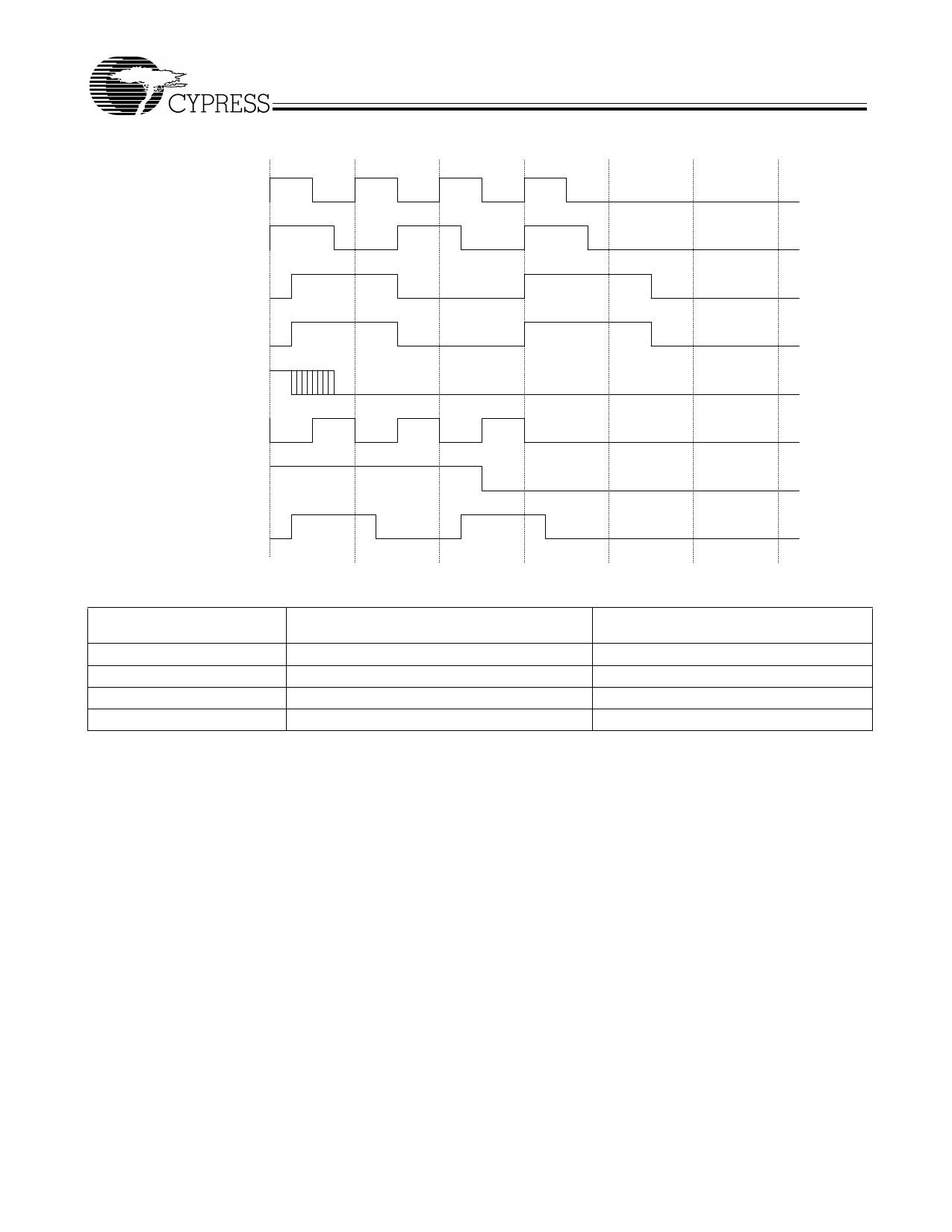
Power Management Timing
0ns
CPU 100 MHz
3V66 66 MHz
PCI 33 MHz
IOAPIC 33 MHz
PD#
SDRAM 100 MHz
10ns
20ns
C9835
30ns
40ns
50ns
60ns
REF 14.3 MHz
VCH_CLK , 48M (0,1)
Table 3. Power Management Current
Figure 1.
Conditions
Power-down (PD# = LOW)
CPU = 66 MHz @ max loads
CPU = 100 MHz @ max loads
CPU = 133 MHz @ max loads
Maximum 2.5V Current Consumption
(VDDC = VDDI = 2.625)
≤ 1mA
60 mA
75 mA
90 mA
Maximum 3.3V Current Consumption
(VDD = AVDD = VDDS = 3.465V)
≤ 1mA
295 mA
295 mA
295 mA
When exiting the power-down mode, the application must started in such a manner as to guarantee that the high pulse
supply power to the VDD pins a minimum of 200 ms before
releasing the PD# pin high to insure that an orderly startup will
occur and that the initial clocks that the device produces are
full and correctly compliant with data sheet specified phase
relationships.
width is a full pulse. Only one rising edge of PCI_F occurs after
the clock control logic is switched for the CPU0 output to
become enabled/disabled.
PCI_STP# Timing
CPU_STP# Timing
CPU_STP# is an input to the clock generator. CPU_STP# is
asserted asynchronously by the external clock control logic
and is internally synchronized to the external PCI_F output. All
other clocks will continue to run while the CPU0 clock is
disabled. The CPU0 is always stopped in a low state and
PCI_STP# is an input to the clock generator and is made
synchronous to the clock driver PCI_F output. It is used to turn
off the PCI clocks for low power operation. PCI clocks are
stopped in a low state and started such that a full high pulse
width is guaranteed. ONLY one rising edge of PCI_F occurs
after the clock control logic switched for the PCI outputs to
become enabled/disabled.
Note:
7. All internal timing is referenced to the CPU clock.
8. CPU_STP# signal is an input signal that is made synchronous to free-running PCI_F.
9. Diagrams shown with respect to 133 MHz. Similar operation when CPU is 100 MHz.
Document #: 38-07303 Rev. **
Page 4 of 18
Share Link: