PDI1394L21 データシートの表示(PDF) - Philips Electronics
部品番号
コンポーネント説明
一致するリスト
PDI1394L21 Datasheet PDF : 52 Pages
| |||
Philips Semiconductors
1394 full duplex AV link layer controller
Preliminary specification
PDI1394L21
Bit 10:
Bit 9:
Bit 6:
Bit 5:
Bit 4:
Bit 3..0:
R/W Cycle Source (CYSOURCE): When asserted, the cycle_count field increments and the cycle_offset field resets for
each positive transition of CYCLEIN. When deasserted, the cycle count field increments when the cycle_offset field
rolls over.
R/W Cycle Timer Enable (CYTIMREN): When asserted, the cycle offset field increments.
R
Transmitter Ready (TxRDY): The transmitter is idle and ready.
R
Root (ROOT): Indicates this device is the root on the bus. This automatically updates after the self_ID phase.
R
Busy Flag (BUSYFLAG): The type of busy acknowledge which will be sent next time an acknowledge is required.
0 = Busy A, 1 = Busy B (only meaningful during a dual-phase busy/retry operation).
R
AT acknowledge received (ATACK): The last acknowledge received by the transmitter in response to a packet sent
from the transmit-FIFO interface while the ATF is selected (diagnostic purposes).
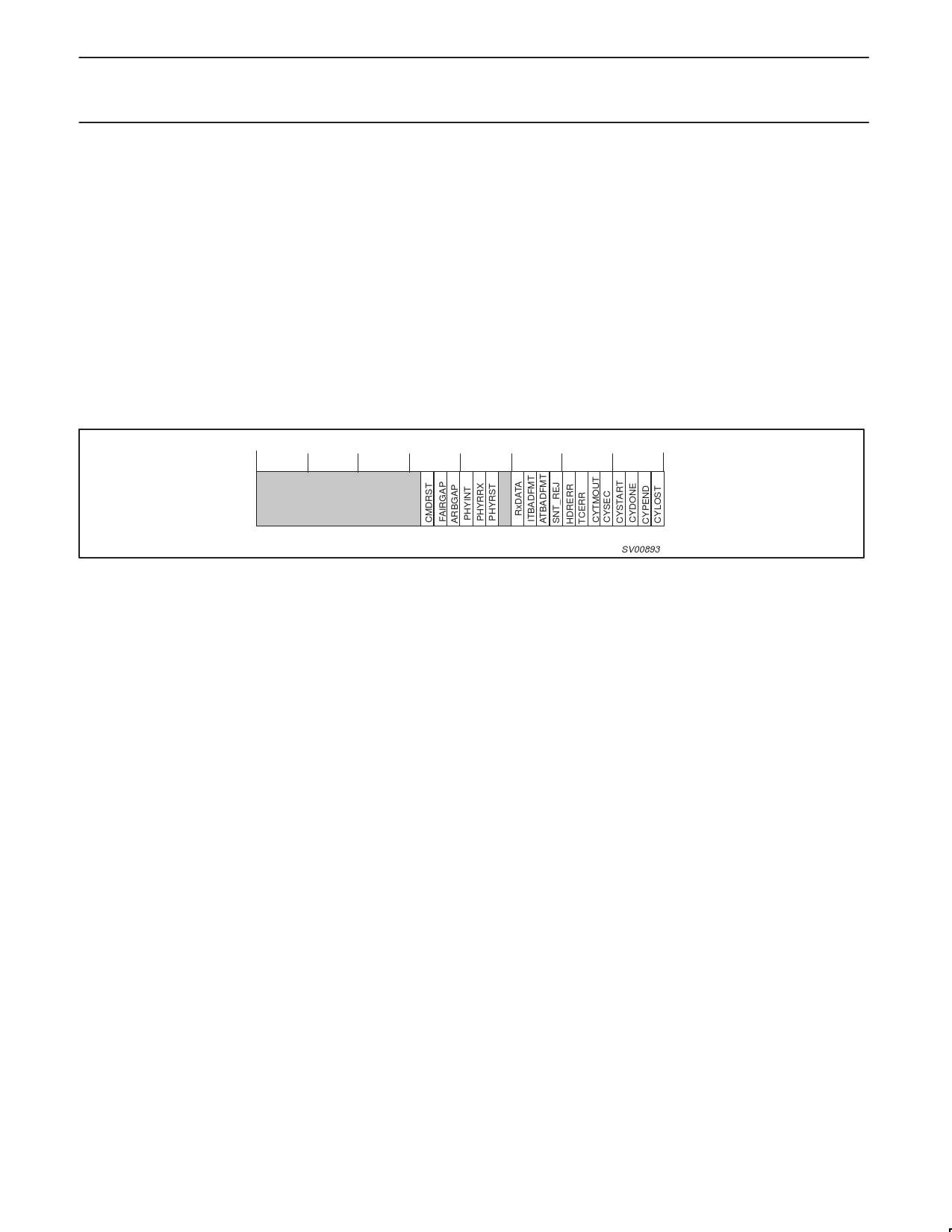
13.1.3 Link /Phy Interrupt Acknowledge (LNKPHYINTACK) – Base Address: 0x008
The Link/Phy Interrupt Acknowledge register indicates various status and error conditions in the Link and Phy which can be programmed to
generate an interrupt. The interrupt enable register (LNKPHYINTE) is a mirror of this register. Acknowledgment of an interrupt is accomplished
by writing a ‘1’ to a bit in this register that is set. This action reset the bit indication to a ‘0’. Writing a ‘1’ to a bit that is already “0” will have no
effect on the register.
31 30 29 28 27 26 25 24 23 22 21 20 19 18 17 16 15 14 13 12 11 10 9 8 7 6 5 4 3 2 1 0
SV00893
Reset Value 0x00000000
Bit 18:
R/W Command Reset Received (CMDRST): A write request to RESET-START has been received.
Bit 17:
R/W Fair Gap (FAIRGAP): The serial bus has been idle for a fair-gap time (called subaction gap in the IEEE 1394
specification).
Bit 16:
R/W Arbitration Reset Gap (ARBGAP): The serial bus has been idle for an arbitration reset gap.
Bit 15:
R/W Phy Chip Int (PHYINT): The Phy chip has signaled an interrupt through the Phy interface. This bit becomes active for
any of the following reasons (1) PHY has detected a loop on the bus, (2) cable power has fallen below the minimum
voltage, (3) the PHY arbitration state machine has timed-out usually indicative of a bus loop, (4) a bus cable has
been disconnected. Typically, recognition and notification of any of the above events by the PHY requires between
166 and 500 microseconds; therefore, this bit is not instantaneously set.
Bit 14:
R/W Phy Register Information Received (PHYRRX): A register has been transferred by the Physical Layer device into the
Link.
Bit 13:
R/W Phy Reset Started (PHYRST): A Phy-layer reconfiguration has started. This interrupt clears the ID valid bit. (Called
Bus Reset in the IEEE 1394 specification).
Bit 11:
R/W Receiver has data (RxDATA): The receiver has confirmed data to the receiver response/request FIFO.
Bit 10:
R/W Isochronous Transmitter is Stuck (ITBADFMT): The transmitter has detected invalid data at the transmit-FIFO
interface when the ITF is selected.
Bit 9:
R/W Asynchronous Transmitter is Stuck (ATBADFMT): The transmitter expected start of new async packet in queue, but
found other data (out of sync with user). Reset to clear.
Bit 8:
R/W Busy Acknowledge Sent by Receiver (SNT_REJ): The receiver was forced to send a busy acknowledge to a packet
addressed to this node because the receiver response/request FIFO overflowed.
Bit 7:
R/W Header Error (HDRERR): The receiver detected a header CRC error on an incoming packet that may have been
addressed to this node.
Bit 6:
R/W Transaction Code Error (TCERR): The transmitter detected an invalid transaction code in the data at the transmit
FIFO interface.
Bit 5:
R/W
Cycle Timed Out (CYTMOUT): ISOCH cycle lasted more than 125µs from Cycle-Start to Fair Gap: Disables cycle
master function
Bit 4:
R/W Cycle Second incremented (CYSEC): The cycle second field in the cycle-timer register incremented. This occurs
approximately every second when the cycle timer is enabled.
Bit 3:
R/W Cycle Started (CYSTART): The transmitter has sent or the receiver has received a cycle start packet.
Bit 2:
R/W Cycle Done (CYDONE): A fair gap has been detected on the bus after the transmission or reception of a cycle start
packet. This indicates that the isochronous cycle is over; Note: Writing a value of ‘0’ to the bit has no effect.
Bit 1:
R/W Cycle Pending (CYPEND): Cycle pending is asserted when cycle timer offset is set to zero (rolled over or reset) and
stays asserted until the isochronous cycle has ended.
Bit 0:
R/W Cycle Lost (CYLOST): The cycle timer has rolled over twice without the reception of a cycle start packet. This only
occurs when cycle master is not asserted.
1999 Aug 06
30
Share Link: 