PDI1394L21 データシートの表示(PDF) - Philips Electronics
部品番号
コンポーネント説明
一致するリスト
PDI1394L21 Datasheet PDF : 52 Pages
| |||
Philips Semiconductors
1394 full duplex AV link layer controller
Preliminary specification
PDI1394L21
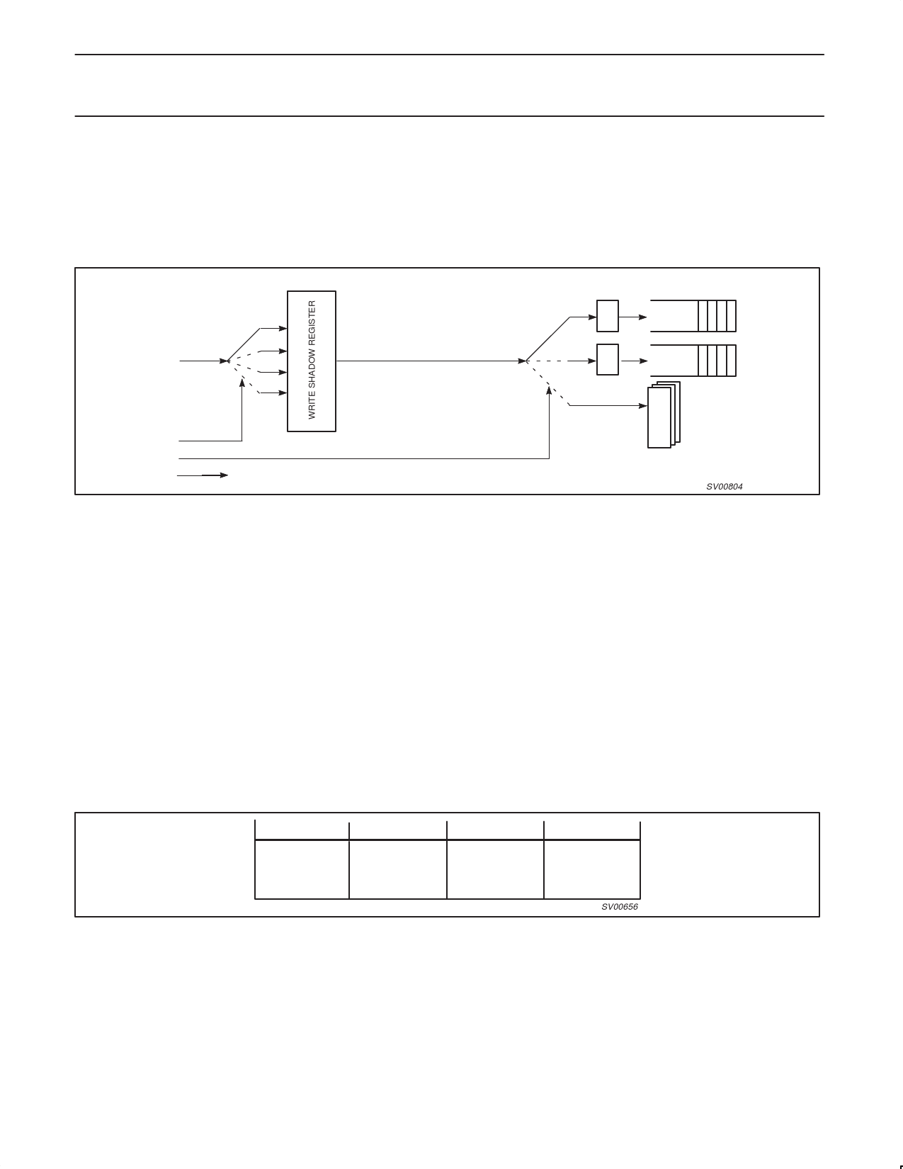
12.3.2 Write accesses
To write to an internal register the host interface must collect the 4 byte values into a 32 bit value and then write the result to the target register
in a single clock tick. This requires a register to hold the 32 bit value being compiled until it is ready to be written to the actual target register.
This temporary register inside the host interface is called the write shadow register. During all write cycles address lines HIF A0 and HIF A1
are used to select which of the 4 bytes of the write shadow register is to be written with the value on the CPU data bus. Only one byte can be
written in a single write access cycle.
MUX
8
32
CPU
TR
MUX
Q
Q
HIF A0..1
REGISTERS
32
HIF A2..7
HIF A8
UPDATE/COPY CONTROL
SV00804
NOTES:
1. It is not required to write all 4 bytes of a register: those bytes that are either reserved (undefined) or don’t care do not have to be written in
which case they will be assigned the value that was left in the corresponding byte of the write shadow register from a previous write
access. For example, to acknowledge an interrupt for the isochronous receiver (external address 0x04C), a single byte write to location
0x100+(0x4C)+3 = 0x14F is sufficient. The value 256 represents setting HIF A8=1. The host interface cannot directly access the FIFOs, but
instead reads from/writes into a transfer register (shown as TR in the Figures above). Data is moved between FIFO and TR by internal logic
as soon as possible without CPU intervention.
2. The update control line does not necessarily have to be connected to the CPU address line HIF A8. This input could also be controlled by
other means, for example a combinatorial circuit that activates the update control line whenever a write access is done for byte 3. This
makes the internal updating automatic for quadlet writing.
3. Writing the bytes of the read shadow register can be done in any order and as often as needed (new writes simply overwrite the old value).
12.3.3 Byte order
The bytes in each quadlet are numbered 0..3 from left (most significant) to right (least significant) as shown in Figure 3. To access a register at
internal address N the CPU should use addresses E:
E=N
; to access the upper 8 bits of the register.
E=N+1
; to access the upper middle 8 bits of the register.
E=N+2
; to access the lower middle 8 bits of the register.
E=N+3
; to access the lower 8 bits of the register.
3130 29 28 27 26 25 24 23 22 21 20 19 18 17 16 15 14 13 12 11 10 9 8 7 6 5 4 3 2 1 0
BYTE 0
BYTE 1
BYTE 2
BYTE 3
SV00656
Figure 3. Byte order in quadlets as implemented in the host interface
12.3.4 Accessing the packet queues
Although entire incoming packets are stored in the receiver buffer memory they are not randomly accessible. These buffers act like FIFOs and
only the frontmost (oldest) data quadlet entry is accessible for reading. Therefore only one location (register address) is allocated to each of the
two receiver queues. Reading this location returns the head entry of the queue, and at the same time removes it from the queue, making the
next stored data quadlet accessible.
With the current host interface such a read is in fact a move operation of the data quadlet from the queue to the read shadow register. Once the
data is copied into the read shadow register it is no longer available in the queue itself so the CPU should always read all 4 bytes before
attempting any other read access (be careful with interrupt handlers for the PDI1394L21!).
1999 Aug 06
11
Share Link: 